In this article I have explained how to use NAND Gates from the IV 4093 or any other similar IC consisting of NAND gates.
About IC 4093
The IC 4093 may not have complicated specifications and attributes yet it proposes many useful utilities. It consists of some fundamental blocks which can be configured according to personal preferences and used for numerous different applications.
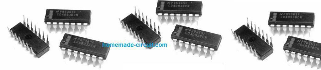
Externally the IC 4093 looks quite an ordinary dual in line type of IC.
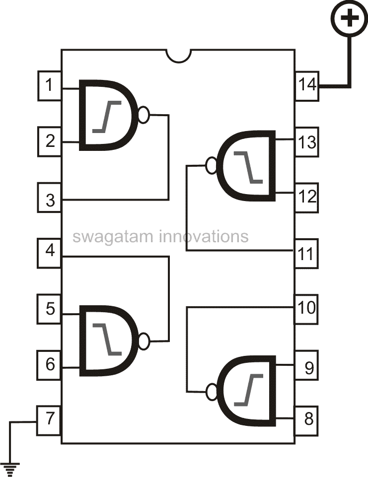
It consists of 14 pins and has four CMOS blocks internally embedded inside its package.
These blocks are called gates, here these are termed NAND gates.
Understanding and using NAND gates of IC 4093 is simple and there’s nothing complicated about these gates.
You can imagine them as an electronic component having a couple of inputs and a single output, quite like a transistor, but these gates are embedded inside a package and are not individual components like transistors.
However the above explained gates are entirely different with their characteristics compared to linear devices like transistors.
The gates are simply made to produce specified sets of output voltages in response to the particular specified sets of input voltage commands.
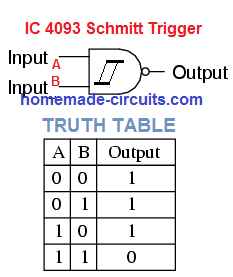
Consider a single NAND gate which will have two inputs and a single output.
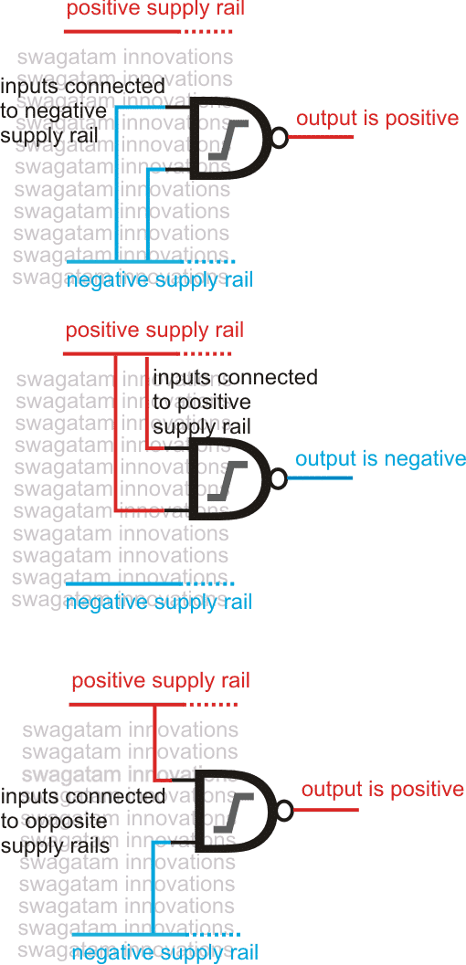
Provide a positive voltage to both the inputs; you get a negative voltage at the output pin.
Apply negative or ground voltages to both the inputs and you get a positive voltage at the output.
Applying opposite voltage levels at the input pins produces no effect on the output and it stays positive with its voltage.
The information tells us about the logical property of the gate that is for a NAND gate, and is generally given in the form of truth tables.
It is important thing to note that the inputs should always be applied with definite voltage levels and cannot be left open.
Absolute Maximum Rating
The following ratings indicate the maximum and the minimum values that must not be exceeded while using the IC 4093, under any circumstances, to avoid permanent damage to the IC
- VDD Supply voltage at pin#14 = -0.5 to +22V
- VI DC input voltage = -0.5 to VDD + 0.5
- II DC input current = ±10 mA
- PD Power dissipation per package = 200 mW
- PD Power dissipation per output transistor = 100 mW
- Top Operating temperature -55 to +125°C
- Tstg Storage temperature -65 to +150
How to Use
The IC 4093 may be used depending on the truth table functions, and the working of the gate outputs in response to gate input logics, or voltages.
The output pin may be normally used for triggering the next stage in an electronic circuit, however it does not carry any criticality and will not damage the IC if left open.
However, the applied voltage to the inputs of the gates should never exceed the supply voltage to the IC which in turn should be within the specified range, normally within 2 to 15 volts.
Undefined voltage levels according to CMOS gates are within 0.75 and 2.5 volts. Anything above 2.5 is considered to be logic 1 or logic high and anything below 0.75 is considered to be a logic 0 or a logic low.
What is Schmitt Trigger
Although the functioning of IC 4093 is exactly same as any ordinary NAND gate, and even the truth table figures are exactly identical, yet the IC 4093 is referred to as schmitt trigger. Why?
It is because, the IC 4093 gate output response to an input signal lags with a small time delay, which ensures that the output is never influenced by accidental, or stray input signal variations, rather the output response are created only to genuine input signals. This function happens due to the internal hysteresis effect attribute of the IC.
For example, suppose a very short momentary pulse is applied to the gate input, which may be just around the threshold of a genuine input logic pulse level.
Such pulses will be ignored by the 4093 schmitt trigger gates, since the slight delay in the output response will cause the gate to wait until the signal is detected to be above the correct thresholds. In this situation the output of the gate will remain stable and unchanged.
The gate output status will change state only once a genuine input pulse is detected, which remains consistently high or low, for the hysteresis delay margin of the gate.
Application Circuits (Learn More)
In the following section we will see how the IC 4093 can be implemented to build a couple of small application circuits.
The first circuit below shows a simple dual LED flasher circuit. The two LEDs blink alternately using just 3 gates of the IC. I have explained more from the following explanation.
Alternate LED Flasher Circuit
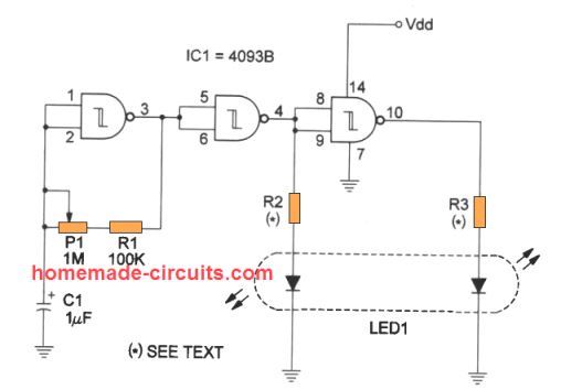
A simple twin alternate LED flasher circuit is shown above using a single IC 4093. The LEDs will flash alternately, and the flashing speed, or the frequency can be adjusted through the P1 pot.
The R2, and R3 will depend on the number of LEDs used, and the supply voltage. These can be set by using the following formula:
R = supply voltage - total LED forward voltage / LED current
for a standard single LED the forward voltage can be assumed to be 3.3V, for 2 in series this will be 6.6 and so on.
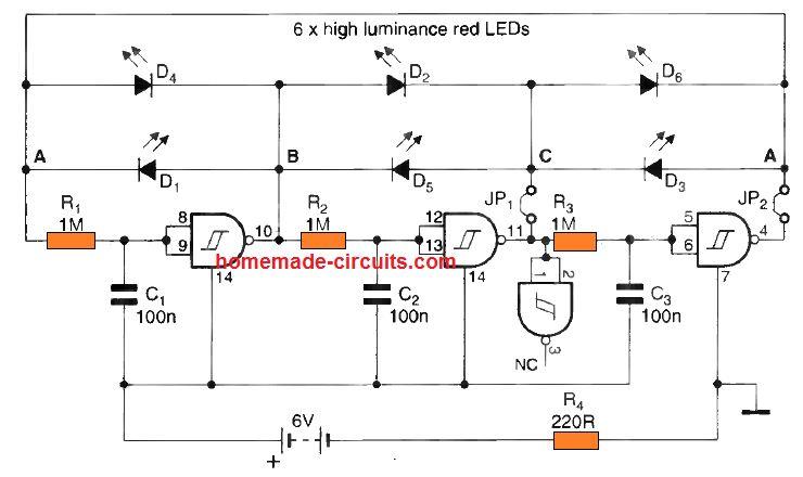
Small Running LED Effect
A small and compact running LED effect can be generated using a single 4093 IC, as shown in the following figure.
The connected LEDs will appear like chasing one after the other in a circle, whose speed will depend on the capacitors C1, C2, C3, and resistors R1, R2, R3.
You can increase or decrease these components to adjust the running frequency of the LEDs.

Comments (21)
Hello Sir, Can you tell me please, the difference between IC CD4047BD & IC CD 4077BE?
Hello Pankaj, IC 4077 is a CMOS quad 2-input Exclusive-NOR Gate while 4047 is an oscillator iC, both are completely different with their function and application.
Hi Mr Swagatam
The LVPS can provids me all the low tensions and:
I could be interested by the first Diagram too but values of parts are missing on the second Diagram neither on the first one
R1, VR1, LDR, R2, R3, D1–D4 for the first Diagram for exemple
R1, R2, P1, T1 for the Second Diagram for exemple
Please tell me how to get them
Thank you for. your patience
Thank you Rabah, I have updated the parts list in the linked article, you can check it out.
If you have any problems, please comment under the linked article, I’ll try to solve your problems there.
Hi Mr SWAGATAM
I’l be very happy if you provide me a schematic of IC 4093 used to swith on special lights when the dark is on and swith them off when the dark is off I mean when I swith ON the lights of my room those special lights comes OFF and vis versa perpetualy.
nota: the special lights are using + 24 V through an LVPS witch is connected to AC line 220V
I wish you anderstand me
good times
Hi Rabah, You can find the design in the second diagram from the following article:
https://www.homemade-circuits.com/how-to-make-light-activated-day-night/
However with 24V input you will have regulate it to 12V for the circuit. The lights can be wired through the relay using the 24V supply sepatately.
Whatever the result you are a MAN a true ONE.
I will give you a summary on my work o, the project once finished and tested
Nice day MAN
Thanks very much for teaching us how to understand and use of 4093. It helps a lot.
Glad it helped you, you can also join our forum for learning in a exclusive manner…
https://www.homemade-circuits.com/community/electronic-circuit-forum/
Thanks a lot Mr swagata i have found most of your post very helpful,i never knew there could be site
You are most welcome Saviour, please keep visiting my site, and feel fee to ask questions whenever required
Dear William, please post the question under the relevant article. so I that i can refer to the diagram and reply
Dear Mr Swagatam, I would like to know which component cuts of the high voltage in your triac voltage stabilizer. Is it the voltage regulator? Thanks and Regards, William Hickman
Can I make this is circuit with transistors. Cause it is not available at my location
what do you intend to make??
Can I make it with transistors?
ant suggestion on what appliance device where i can find this IC 4093? coz it aint available here in electronic shops. thank you
this IC can have a huge range of applications and configurations, so it cannot be predicted which appliance might be using this IC
ive been googling all the time on what appliances that uses IC 4093 coz it is not available in electronics store here and maybe it would be much more easy if can find one appliance/device
Thank you sir
Sir I want to know about inver circuit design