IC 4018 is a 16-pin CMOS presettable divide-by-N counter, also known as a binary counter. It is commonly used in digital electronics for frequency division and timing applications.
Description
The IC 4018 family includes 5 Johnson-Counter stages, buffered Q outputs from each stage, and counter preset control gating. There are CLOCK, RESET, DATA, PRESET ENABLE, and 5 separate JAM inputs.
Divide by 10, 8, 6, 4, or 2 counter combinations could be achieved by supplying the Q5, Q4, Q3, Q2, Q1 signals back to the DATA input, in that order.
By using a CD4011B to gate the feedback connection to the DATA input, you may build divide-by-9, 7, 5, or 3 counter arrangements. Several CD4018BMS units could be used to create divide-by functions bigger than ten.
During the positive clock-signal transition, the counter advances one count. On the clock line, Schmitt Trigger action allows for infinite clock rise and fall times.
A high RESET signal resets the counter to an all-zero state. A high PRESET-ENABLE signal permits data from the JAM inputs to be used to preset the counter. To ensure the right counting sequence, anti-lock gating is given.
Features:
- Supply voltage range: 3V to 18V
- Low power consumption: typically 10µA at 5V
- Operating temperature range: -55°C to +125°C
- High noise immunity: 0.45Vdd typ.
- Schmitt-trigger input circuitry for noise immunity
- Output capability: standard and high-speed (TC output)
- Pin-compatible with other 4000-series CMOS devices
Pinout Description
The pinout details of the IC 4018 can be seen in the following figure:
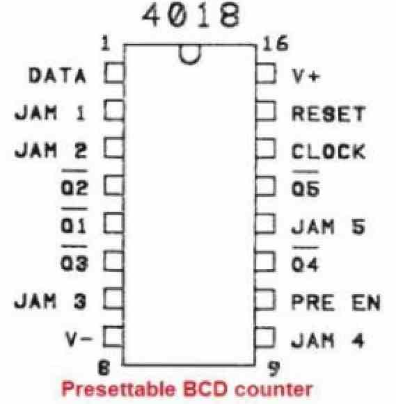
The IC 4018 is a 4-bit binary counter with a maximum count of 16 (2^4). It can be preset to any value between 0 and 15 using the four preset inputs (Q1-Q4).
The clock input is used to advance the counter by one count on the rising edge of each clock pulse. The clock enable input (Pre EN) and output enable input (OE) are used to enable or disable the clock and output signals, respectively.
The master reset input (MR) is used to clear the counter to zero when pulled low. The carry output (TC) goes high when the counter reaches its maximum count, and can be used to cascade multiple counters for higher counting capability.
Applications:
- Frequency division and timing circuits
- Digital clocks and timers
- Industrial control systems
- Measurement and instrumentation systems
- Counting and sequencing circuits
How to Use the JAM Inputs for Programmable Divide by N Operation
The CD4018 IC has five individual JAM inputs which allow us to preset it five internal counter stage to required logic condition.
These input is useful when we want to build programmable frequency divider instead of using only the fixed divide by 2, then 4, 6, 8 or 10 configurations.
However the JAM inputs do not work like ordinary binary selection inputs.
We cannot simply apply the binary equivalent of a number to JAM1 through JAM5 and expect the IC to divide by that number. 1.
Understanding the JAM Inputs
The five JAM inputs are associated with five internal Johnson counter stage. Each JAM input determines the preset condition of its corresponding stage.
To load the JAM conditions, we have to momentarily make PRESET ENABLE (pin 10) HIGH.
During this condition, logic level applied to JAM1 through JAM5 are transferred to the respective counter stages.
After the required conditions are loaded, PRESET ENABLE is returned LOW, allowing counter to resume its normal counting operation.
The RESET input (pin 15) performs a different function. When RESET is made HIGH, then all the counter stages is cleared to their initial zero condition.
Therefore we must understand the difference between these two inputs:
RESET: Clears all five counter stage.
PRESET ENABLE: Loads the five counter stage according to the JAM input condition. 2. How to Obtain a Required Divide by N Ratio To obtain a particular divide by N ratio, we must configure feedback connection so that counter repeats it counting sequence after required number of clock pulses.
Basic procedure is as follow: Decide required division ratio, like divide by 5, divide by 7 or divide by 9. Determine the counter state in which the counting sequence must repeat, configure the feedback logic using the appropriate Q output.
If a preset based sequence is required, then apply the necessary logic condition to JAM1 through JAM5. Use PRESET ENABLE to load these conditions at the required point in counting sequence.
The counter then repeat same sequence, producing required frequency division.
Output frequency is determined by number of input clock pulses required to complete one complete counting cycle.
Therefore: Output Frequency = Input Clock Frequency / N 3. Example: Divide by 7 Using CD4018
Texas Instruments datasheet provides practical divide by 7 circuit using a CD4018 and a CD4011 NAND gate.
In this arrangement, Q3 and Q4 outputs are connected to NAND gate and its output is inverted before being fed back to the DATA input. This feedback arrangement makes CD4018 skip the unwanted counter state and repeat its counting sequence after seven clock pulse.
Interestingly, this particular divide by 7 example does not use the JAM inputs to select the division ratio.
JAM inputs are simply connected to ground in the illustrated circuit.
This is an important point: the feedback logic establishes the division ratio, while the JAM inputs provide the facility to preset counter stages when a different starting or repeating state is required then.
Can We Obtain Any Divide by N Ratio?
Yes, the CD4018 can be used for programmable divide by N applications but the required external logic must be designed according to the desired counting sequence.
For divide by 2, 4, 6, 8 and 10, the appropriate counter output can be connected directly back to the DATA input.
For divide by 3, 5, 7 and 9, additional gating using a CD4011 is required, as shown in datasheet.
For larger division ratios, multiple CD4018 ICs can be cascaded.
When using the JAM input for a programmable divider, then the preset conditions and the feedback logic must be designed together.
There is no simple universal binary to JAM conversion formula for selecting division ratio.
Thus CD4018 provide a flexible way of constructing fixed and programmable frequency divider using its internal Johnson counter stage, preset facility and suitable external feedback logic.

Questions & Answers
You have given just what is available in data sheet. Can you explain how to divide by N using Jam inputs?
The five JAM inputs are used to preset the internal counter stages to a desired starting condition. To do this, apply the required HIGH or LOW logic levels to JAM1–JAM5 and momentarily make PRESET ENABLE (pin 10) HIGH. Then return PRESET ENABLE LOW to resume normal counting. However, for a specific divide-by-N ratio, the feedback connection and external logic must also be configured accordingly. The JAM inputs alone do not determine the division ratio.