So now we are talking about this digital IC called 4035 which is made using CMOS technology, that means it will use very low current and will give us high noise immunity. Inside this IC we have got 4 flip-flops which are arranged in such a way that they can hold and shift 4-bit data. We call it a 4-bit register and also we call it parallel-in parallel-out shift register because we can put all 4 bits of data together at once, and also take them out together from 4 output pins.
Now the good part is that, this IC can do multiple things. We can use it to store data, or we can use it to shift the data left or right and we can also connect more such ICs to make longer chains. So it becomes very useful in many logic circuits, where we want to delay data or convert parallel data to serial data, or opposite.
Main Features of IC 4035:
| Feature | Description |
|---|---|
| Technology | CMOS (low power, high noise immunity) |
| Bit count | 4 bits |
| Shift Direction | Left or Right (selectable) |
| Inputs | Parallel Data Inputs (D1 to D4), Clock, Mode Control, Reset |
| Outputs | Parallel Outputs (Q1 to Q4) |
| Package Type | DIP-16, SOIC-16 |
| Operating Voltage Range | 3V to 15V (typically used at 5V or 12V) |
| Static Power Consumption | Very low (only leakage current) |
| Propagation Delay | About 200ns to 600ns depending on voltage |
Pin Diagram and Pinout Details:

So now we see that IC 4035 is normally available in 16-pin DIP package. Here is how the pins are connected:
| Pin No. | Pin Name | Function / Description |
|---|---|---|
| 1 | Q1 / Q1(bar) | Output pin for bit 1 (both normal and inverted, depending on True/Comp pin) |
| 2 | True / Comp. | Selects whether outputs are true (non-inverted) or complement (inverted) |
| 3 | K (bar) | Serial input for shifting left (active low control) |
| 4 | J | Serial input for shifting right |
| 5 | Reset | Asynchronous reset input (clears all outputs when HIGH) |
| 6 | Clock | Main clock input (positive edge triggered) |
| 7 | P/S | Parallel / Serial mode selector (HIGH = Parallel load, LOW = Shift mode) |
| 8 | VSS | Ground (0V) |
| 9 | PI1 | Parallel data input for bit 1 (Q1) |
| 10 | PI2 | Parallel data input for bit 2 (Q2) |
| 11 | PI3 | Parallel data input for bit 3 (Q3) |
| 12 | PI4 | Parallel data input for bit 4 (Q4) |
| 13 | Q4 / Q4(bar) | Output for bit 4 (with complement selection) |
| 14 | Q3 / Q3(bar) | Output for bit 3 (with complement selection) |
| 15 | Q2 / Q2(bar) | Output for bit 2 (with complement selection) |
| 16 | VDD | Positive supply voltage (typically +5V to +15V) |
Electrical Characteristics:
| Parameter | Min | Max | Unit | Notes |
|---|---|---|---|---|
| Supply Voltage VDD | 3 | 15 | Volts | Normally 5V or 12V |
| Input HIGH voltage (VIH) | 0.7 × VDD | - | Volts | To detect HIGH |
| Input LOW voltage (VIL) | - | 0.3 × VDD | Volts | To detect LOW |
| Output HIGH (VOH) | 0.95 × VDD | - | Volts | At very low current |
| Output LOW (VOL) | - | 0.05 × VDD | Volts | At very low current |
| Max Clock Frequency | ~1 to 8 MHz | Hertz | Depends on VDD | |
| Input Current | -1 | +1 | µA | Very low |
Working Modes and Truth Table:
So now we have to understand that IC 4035 can do mainly two jobs:
- Load data in all 4 flip-flops at once (parallel load)
- Shift data left or right one bit per clock
For this, we have 3 control inputs:
- Reset – clears everything
- Shift/Load – decides whether we are loading or shifting
- Direction – decides shift-left or shift-right
Now here is the simplified truth table:
| Reset | Shift/Load | Clock ↑ | Direction | Operation |
|---|---|---|---|---|
| 1 | X | X | X | All Q = 0 (Reset state) |
| 0 | 0 | ↑ | X | Load D1 to D4 into Q1-Q4 |
| 0 | 1 | ↑ | 1 | Shift Left (Qn = Qn+1) |
| 0 | 1 | ↑ | 0 | Shift Right (Qn = Qn−1) |
So we apply clock pulses, and depending on whether Shift/Load is HIGH or LOW, the IC will either shift or load. Also, direction tells us where the shifting will happen.
How this IC 4035 looks and works from outside
This IC comes in a 16-pin package, most commonly in DIP type which is easy to use on breadboard and normal circuits. Now from outside it looks like a normal IC but from inside it has 4 flip-flops, clock circuit, mode control circuit and some control logic. Every flip-flop has one data input and one data output. So in total we have 4 data inputs and 4 data outputs. And along with that, we have some extra control pins, like clock, reset, shift/load and direction pin.
Power supply pins and basic working condition
Now to make this IC work, first we have to give proper power supply. It has one pin called VDD where we connect positive voltage, that can be from 3V to 15V but normally we use either 5V or 12V, depending on rest of the circuit. Then there is VSS pin, that is ground or 0V. So once we connect proper power, the IC is ready to work.
Understanding the Data Inputs and Outputs
So now let us talk about the data inputs. This IC has four parallel inputs called D1, D2, D3, and D4. These are used to give 4 bits of data at once to the internal flip-flops. We just put the binary values (0 or 1) on these four pins, and then when we give the clock pulse with proper control pins, the data gets loaded into the flip-flops. The loaded values then appear on the outputs which are called Q1, Q2, Q3, and Q4. These are the main output pins of the four flip-flops.
So for example if we give 1 to D1, 0 to D2, 1 to D3, and 0 to D4 and if we trigger the clock in correct load mode, then we will see 1, 0, 1, 0 appearing at Q1 to Q4. That is how it works in loading mode.
Understanding the Clock Pin
Now the main working of the flip-flops happen during the clock pulse. There is a Clock pin in this IC, where we give the square wave signal. This IC is edge-triggered, that means it will react only on the rising edge of the clock, not during high or low level. So every time clock goes from LOW to HIGH, that is called rising edge, the IC will perform one action like loading or shifting, depending on what mode we are keeping it.
Reset Pin Function
Now if we make Reset pin = HIGH, no matter what other pins are doing, then all flip-flops will go LOW, that means:
- Q1 = 0
- Q2 = 0
- Q3 = 0
- Q4 = 0
As soon as reset becomes LOW again, we can start working normally.
So, this IC has a Reset pin and this one is very simple to understand. If we apply a logic HIGH to this Reset pin then all flip-flops inside the IC will immediately become 0, that means Q1 to Q4 will become 0, no matter what data was there. So whenever we want to clean or clear the register, then we can just give a HIGH to Reset pin. Once reset is done, then we can bring it LOW again and normal operation can continue.
Shift/Load Control Pin
Now this pin is very important, and it decides what kind of job the IC will do. It is called Shift/Load pin. If we give LOW logic on this pin then the IC will go into Load Mode. In this mode when we give a clock pulse, then the IC will take the D1 to D4 inputs and load them into the flip-flops. So basically, if we want to load fresh 4-bit data, then we must keep Shift/Load pin LOW and then give clock pulse.
But if we make Shift/Load pin HIGH, then the IC will go into Shift Mode. In this mode, when we give clock pulses, then data inside the flip-flops will shift by one bit position. So the data in Q1 will go to Q2, Q2 to Q3, Q3 to Q4 and so on. But for this to work properly, we must also tell the IC in which direction to shift. That is done using another control pin called Direction.
Direction Pin Function
Now let us see what this Direction pin does. This pin decides whether the shifting will go Left or Right. If we give LOW to Direction pin then the IC will shift data towards right, that means Q4 will take value from Q3, Q3 from Q2 and so on. Q1 will take new value from a pin called Serial Input.
If we give HIGH to Direction pin then the data will shift towards left, that means Q1 will take value from Q2, Q2 from Q3 and so on. Q4 will then take new value from Serial Input.
So depending on Direction pin, the Serial In data will go to either Q1 or Q4.
Serial Input Pin
Now the Serial In pin is used only when we are in shift mode. When we are shifting left or right, we always need one new bit to come from outside. That new bit comes from this Serial In pin. So if we are shifting right, then bit from Serial In will go to Q1 and if we are shifting left, it will go to Q4.
So in serial shifting, this pin becomes very important because otherwise shifting will just push in zeros.
A Simple Working Example
Suppose we load 1010 into D1 to D4. So we keep Shift/Load = LOW, Direction can be anything, we give clock pulse and Q1 to Q4 will become 1010.
Now we want to shift this data towards right. So we make Shift/Load = HIGH, Direction = LOW (means right shift) and Serial In = 1. Then we give clock pulse.
After one shift, data becomes:
- Q1 = 1 (from Serial In)
- Q2 = 1 (from Q1)
- Q3 = 0 (from Q2)
- Q4 = 1 (from Q3)
We can keep shifting again and again like this. Same thing works in left shift, but direction pin must be HIGH.
How the Shifting Happens
Let us say now the flip-flops store this:
Q1 = 1, Q2 = 0, Q3 = 1, Q4 = 1
If we now give:
- Shift/Load = 1 (shift mode)
- Direction = 0 (right shift)
- Clock ↑ (rising edge pulse)
Then data moves like this:
- Q4 becomes Q3 (1)
- Q3 becomes Q2 (0)
- Q2 becomes Q1 (1)
- Q1 takes new value from Serial In pin
So if Serial In = 0, then new values after shift will be:
- Q1 = 0
- Q2 = 1
- Q3 = 0
- Q4 = 1
Same way if direction = 1 (left), then shifting will go opposite.
Timing and Speed
This IC works with clock frequencies up to around 1 MHz to 8 MHz, depending on what voltage we are giving. If voltage is higher, like 15V, then speed also becomes higher. But still this is not super fast. We can use it comfortably in normal digital circuits, not in high-speed systems.
The delay between input and output which we call propagation delay, can be around 200 to 600 nanoseconds, depending on voltage.
How much current and voltage it needs
So this IC works best between 3V to 15V and it takes almost no current because CMOS design only draws power when switching. So static current is in nanoampere range. The input pins do not take any current because inputs are high impedance. The output pins can give or sink only few mA maybe 1 or 2 mA safely. So we should not connect big loads directly on outputs. If we want to drive LEDs or relays, we must use transistor buffer.
Application Circuits:
We can use this IC in many places like:
- Temporary data storage
- Data shifting and delaying
- Serial to Parallel conversion
- Parallel to Serial conversion
- Keyboard encoder
- Display drivers
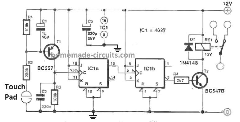
Example Circuit Application of IC 4035 for Generating 3-Phase Signal Output

Where we can use this IC 4035
We can use this IC in many useful circuits. Some examples are:
We can use it in parallel to serial conversion where we load 4-bit data and then shift it out one bit at a time using clock pulses.
Or we can use it in serial to parallel conversion, where we keep giving 1-bit data through Serial In and shift it inside and finally read all 4 outputs together.
We can also use this IC as a temporary 4-bit data register, where we just load and hold the data.
We can use it for delay lines, like creating time delays for digital pulses.
We can also use it in keyboard scanning, digital display and many microcontroller interface designs.
If we need more than 4 bits then we can connect multiple 4035 ICs in series. That means Q4 of first IC can go to Serial In of second IC. Clock and control pins can be common. So we can make 8-bit or 12-bit or longer shift register chain.
Example Connection for Parallel Load:
Let us say we want to load 1010 into Q1 to Q4.
- D1 = 1
- D2 = 0
- D3 = 1
- D4 = 0
- Shift/Load = 0 (Load mode)
- Clock ↑
→ Now Q1 to Q4 will become 1010
Example for Shift Register Chain:
We can also connect 2 or more 4035 ICs to make an 8-bit or longer shift register.
For example:
- Q4 of first IC connects to Serial In of second IC.
- Clock and control pins connected same for both.
- So shifting will propagate from first IC to second IC.
Important Notes:
- Clock must be clean square wave, not slow rise time.
- All unused inputs must be tied to VDD or GND, not left floating.
- Reset must be LOW to allow normal operation.
- For shifting, clock rising edge must be used.
- Shift/Load pin decides mode, must be stable before clocking.
Package Types:
- DIP-16 (Dual Inline Package)
- SOIC-16 (Surface mount)
Pin layout is same in both.
Final Thoughts
So this IC 4035 is like a small digital brain that can hold, load, and shift 4-bit data. It is very flexible because it supports both shifting and loading and shifting can be in both directions which is not available in many other registers. It is very power efficient and also easy to use. We just need to manage the control pins properly, that is, clock, reset, shift/load, direction and serial in.
If we understand the truth table and how to give clock pulses then using this IC becomes very easy and fun. And because it is CMOS so we can use it in both 5V logic circuits and also 12V logic systems.

Comments (2)
I find it difficult setting this ic4035 for three phase oscillator ,it does not produce any output following the schematic
Please disconnect pin10 and pin12 from ground and connect them with pin16 and pin2 and check the response…