If you have understood correctly, how to use transistors in circuits, you might have already conquered half of electronics and its principles. In this post we make an effort in this direction.
Introduction
Transistors are 3 terminal semiconductor devices which is able to conduct relatively high power across their two terminals, in response to a significantly low power input at the third terminal.
Transistors are basically of two types: bipolar junction transistor (BJT), and metal–oxide–semiconductor field-effect transistor (MOSFET)
For a BJT, the 3 terminals are designated as base, emitter, collector. A low power signal across base/emitter terminal allows the transistor to switch a comparatively high power load across its collector terminal.
For MOSFETs these are designated as Gate, Source, Drain. A low power signal across Gate/Source terminal allows the transistor to switch a comparatively high power load across its collector terminal.
For the sake of simplicity we will discuss BJTs here, since their charcaeritics is less complex compared to MOSFETs.
Transistors (BJTs) are the building blocks of all semiconductor devices found today. If there wouldn’t be transistors there wouldn’t be any ICs or any other semiconductor component. Even ICs are made up of 1000s of closely knit transistors which constitute the features of the particular chip.
New electronic hobbyists usually find it difficult to handle these useful components and configure them as circuits for an intended application.
Here we’ll study the functions and the way of handling and implementing bipolar transistors into practical circuits.
How to use Transistors like a Switch
Bipolar transistors are generally a three lead active electronic component which fundamentally work as a switch for either switching ON or switching OFF power to an external load or an associated electronic stage of the circuit.
A classic example can be seen below, where a transistor is connected as a common emitter amplifier:
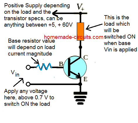
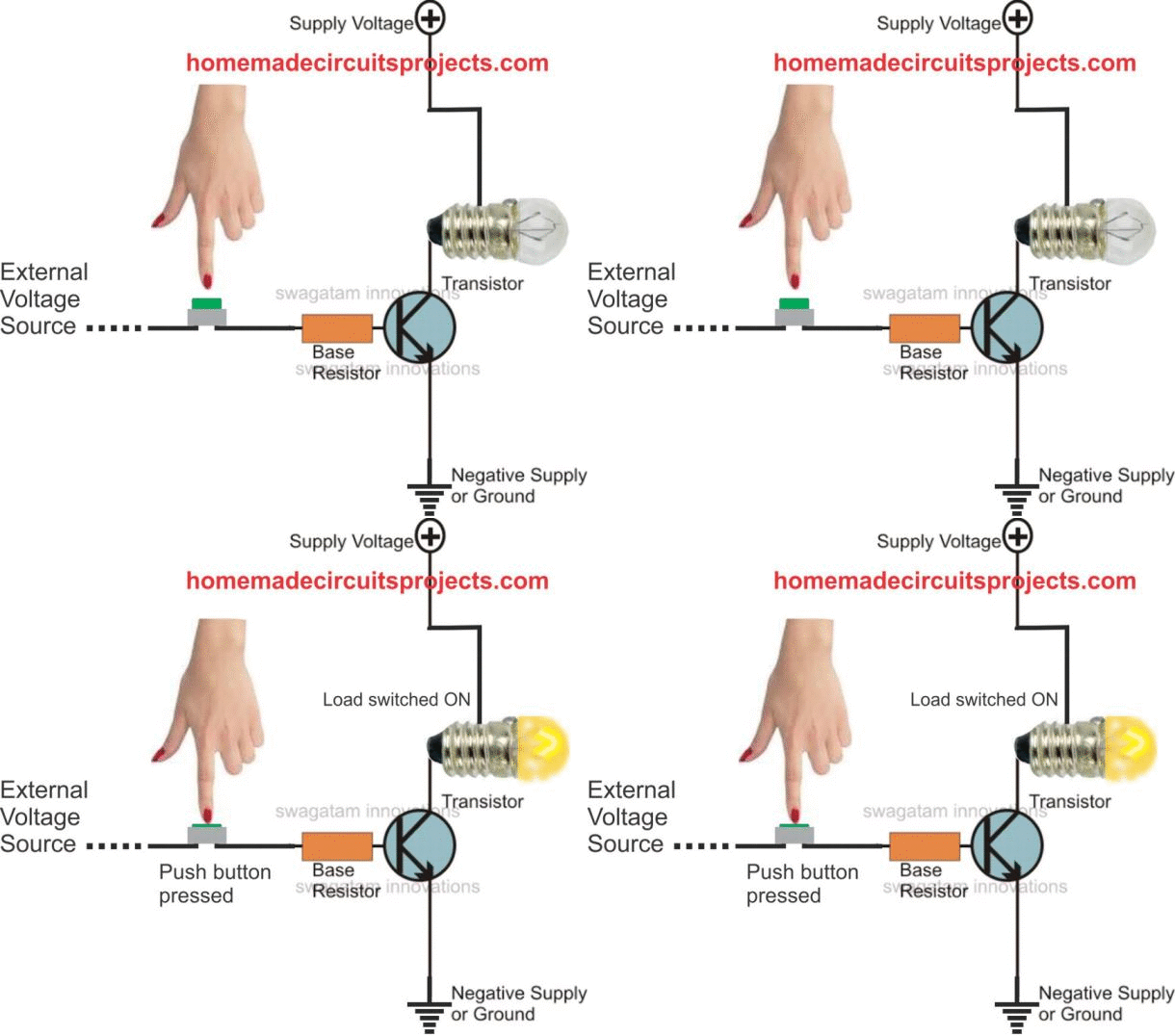
This is the standard method of using any transistor like a switch for controlling a given load. You can see when a small external voltage is applied to the base, the transistor switches ON and conducts heavier current across the collector emitter terminals, switching on a bigger load.
The base resistor value can be calculated using the formula:
Rb = (Base Supply Vb - Base-Emitter Forward Voltage) x hFE / Load Current
Also remember that, the negative or the ground line of the external voltage must be connected with the transistor ground line or the emitter, otherwise the external voltage will have no effect on the transistor.
Using Transistor as a Relay Driver
I have already explained in one of my earlier posts regarding how to make a transistor driver circuit.
Basically it uses the same configuration as shown above. Here's the standard circuit for the same:
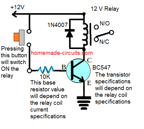
If you are confused about the relay, you can refer to this comprehensive article which explains everything about relay configurations.
Using Transistor to Light Dimmer
The following configuration shows how a transistor can be used as a light dimmer using a emitter follower circuit.
You can see as the variable resistor or the pot is varied, the lamp intensity also varies. We call it emitter-follower, because the voltage at the emitter or across the bulb follows the voltage at the base of the transistor.
To be precise the emitter voltage will be just 0.7 V behind the base voltage. For example, if the base voltage is 6 V, the emitter will 6 - 0.7 = 5.3 V and so on. The 0.7 V difference is due to the minimum forward voltage drop rating of the transistor across the base emitter.
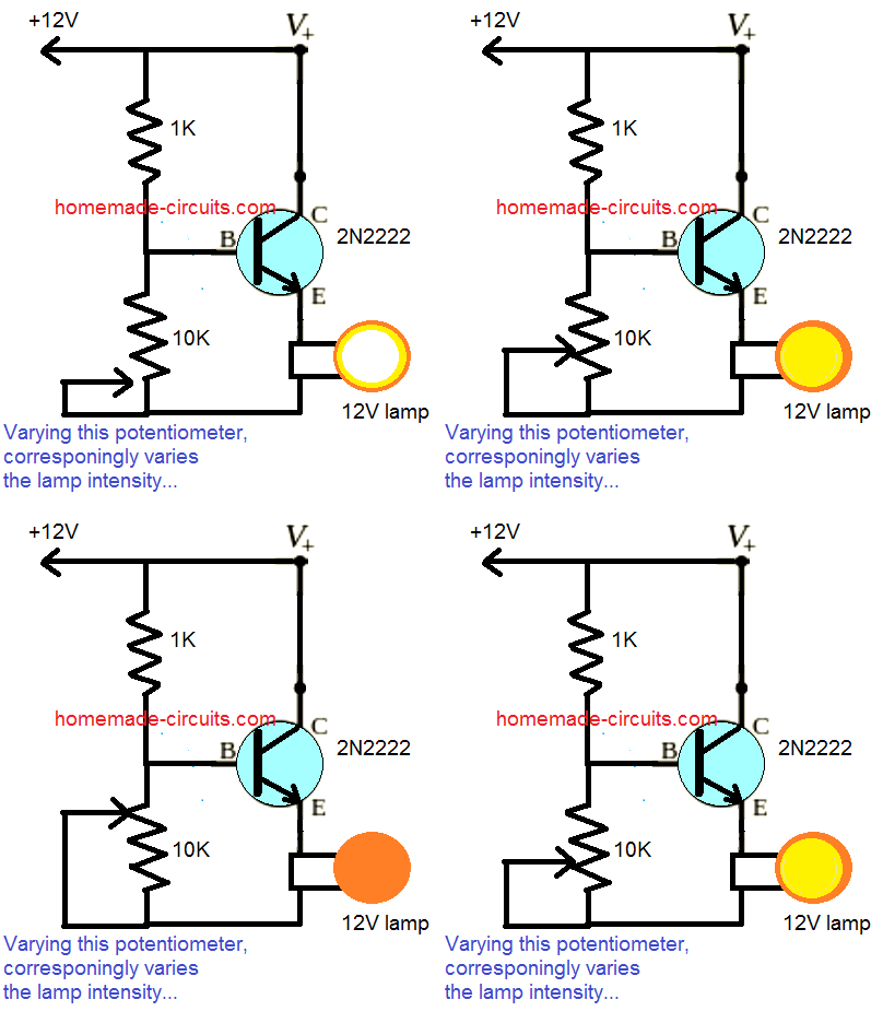
Here, the pot resistance along with the 1 K resistor forms a resistive divider network at the base of the transistor. As the pot slider is moved, the voltage at the base of the transistor is changed, and this correspondingly alters the emitter voltage across the lamp, and the lamp intensity changes accordingly.
Using Transistor as a Sensor
From the above discussions you might have observed that the transistor is doing one crucial thing in all the applications. It is basically amplifying the voltage at its base by allowing a large current to be switched across its collector emitter.
This amplifying feature is also exploited when a transistor is used as a sensor. The following example shows how it can used to sense the difference in ambient light, and switch ON/OFF a relay accordingly.
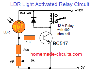
Here too the LDR and the 300 ohm/5 k preset forms a potential divider at the base of the transistor.
The 300 ohm is actually not required. It is included to ensure that the transistor base is never fully grounded, and thus it is never completely disabled or shut off. It also ensures that the current through the LDR can never exceed a certain minimum limit, no matter how bright the light intensity is on the LDR.
When it's dark, the LDR has a high resistance which is many times higher than the combined value of the 300 ohm and the 5 K preset.
Due to this the transistor base gets more ground side voltage (negative) than the positive voltage, and its collector/emitter conduction remains switched OFF.
However when sufficient light falls on the LDR, its resistance drops to a few kilo-ohm value.
This enables the base voltage of the transistor to rise well over the 0.7 V mark. The transistor now gets biased and switches ON the collector load, that is the relay.
As you can see, in this application too the transistors is basically amplifying the tiny base voltage such that a bigger load at its collector could be switched ON.
The LDR can be replaced with other sensors such as a thermistor for heat sensing, a water sensor for water sensing, a photodiode for IR beam sensing, and so forth.
Question for you: What happens if the position of the LDR and the 300/5 K preset are swapped with each other?
Transistor Packages
Transistors are normally recognized by their external package in which the particular device may be embedded. The most common types of package in which these useful devices are enclosed, are the T0-92, TO-126, TO-220 and TO-3. We will try to understand all these specifications of transistors and also learn how to use them in practical circuits.
Understanding Small Signal TO-92 Transistors:
Transistors like BC547, BC557, BC546, BC548, BC549, etc all come under this category.
These are the most elementary in the group and are used for applications involving low voltages and currents. Interestingly this category of transistors is used most extensively and universally in electronic circuits due to their versatile parameters.
Normally these devices are designed to handle voltages anywhere between 30 to 60 volts across their collector and emitter.
The base voltage is not more than 6, but they can be easily triggered with a voltage level as low as 0.7 volts at their base. However the current must be limited to 3 mA approximately.
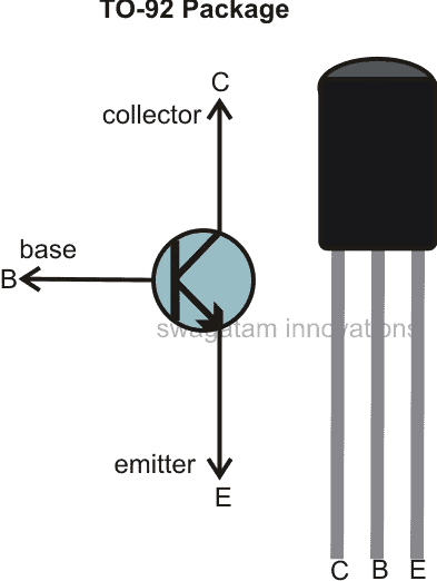
The three leads of a TO-92 transistor may be identified in the following manner:
Keeping the printed side toward us, the right side lead is the emitter, the center one is the base and the left hand side leg is the collector of the device.
UPDATE: Want to know how to use transistors with Arduino? Read it here
How to Configure a TO-92 Transistor into Practical The Designs
Transistors are mainly of two types, an NPN type and a PNP type, both are complementary to each other. Basically they both behave the same way but in the opposite references and directions.
For example an NPN device will require a positive trigger with respect to the ground while a PNP device will require a negative trigger with reference to a positive supply line for implementing the specified results.
The three leads of the transistor explained above needs to be assigned with specified inputs and outputs for making it work for a particular application which obviously is for switching a parameter.
The leads need to be assigned with the following input and output parameters:
The emitter of any transistor is the reference pinout of the device, meaning it needs to be assigned the specified common supply reference so that the remaining two leads can operate with reference to it.
An NPN transistor will always need a negative supply as the reference, connected at its emitter lead for proper functioning, while for a PNP, it will be the positive supply line for its emitter.
The collector is the load carrying lead of a transistor and the load which needs to be switched is introduced at the collector of a transistor (see figure).
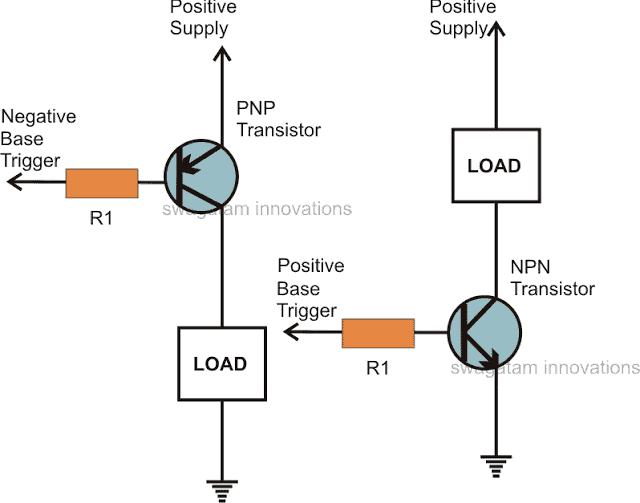
The base of a transistor is the trigger terminal which is required to be applied with a small voltage level so the current through the load can pass through, across to the emitter line making the circuit complete and operating the load.
The removal of the trigger supply to the base immediately switches OFF the load or simply the current across the collector and the emitter terminals.
Understanding TO-126, TO-220 Power Transistors:
These are medium type of power transistors used for applications which require switching of powerful relatively powerful loads lie transformers, lamps etc. and for driving TO-3 devices, typical egs are BD139, BD140, BD135 etc.
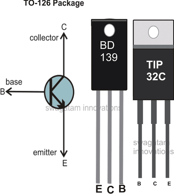
Identifying BJT pinouts
The pinout are identified in the following manner:
Holding the device with its printed surface facing you, the right side lead is the emitter, the center lead is the collector and the left side lead is the base.
The functioning and the triggering principle is exactly similar to what is explained in the previous section.
The device is operated with loads anywhere from 100 mA to 2 amps across their collector to emitter.
The base trigger can be anywhere from 1 to 5 volts with currents not exceeding 50 mA depending upon the power of the loads to be switched.
Understanding TO-3 Power Transistors:
These can be seen in metallic packages as shown in the figure. The common examples of TO-3 power transistors are 2N3055, AD149, BU205, etc.
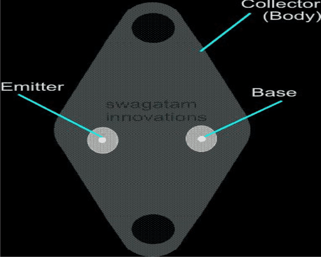
The leads of a TO-3 package can be identified as follows:
Holding the lead side of the device toward you such that the metal part beside the leads having larger area is held upward (see figure), the right side lead is the base, the left side lead is the emitter while the metallic body of the device forms the collector of the package.
The function and operating principle is just about the same as explained for the small signal transistor however the power specs increase proportionately as given below:
Collector-emitter voltage can be anywhere between 30 to 400 volts and current between 10 to 30 Amps.
Base trigger should be optimally around 5 volts, with current levels from 10 to 50 mA depending upon the magnitude of the load to be triggered. The base triggering current is directly proportional to the load current.
Have more specific questions? Please ask them through your comments, I am here to solve them all for you.
Comments
I am a follower of your inventions. If any day I seek help for PCBs of your circuit can you help me out by providing PCBs with your terms and conditions?
Thank you Soubhik, However designing PCBs can be highly time consuming so it may not be possible for me to design PCB for you due to lack of time.
What are some more applications for transistors
Please
I need basic circuit tutorials in pdf format
Sorry I do not have a pdf format, I have them in online article format only
Would you kindly help me use NPN transistor in DC-sensing circuit? I have about (20) 2N2222A available.
In my car, the dash cluster LED for parking brake normally gets switched earth connection…but I need to have switched 12V instead. The new parking module sends out 12V signal and expects 8mA load. Can I arrange resistors on base & emitter to have 8mA load and saturate the BJT to turn on the dash cluster LED?
In all modern vehicles, all the electrical loads are connected with the common ground, meaning one end of all the gadgets will be permanently connected to the ground line….so in your car too the LEDs are referenced to the ground line….you are saying that you want your LED to be switched from the +12V line instead the ground line….is that right?
If I have understood it right, the first circuit is all that you need, the LEDs may be shifted to the transistor collector side, and the base of the transistor switched from the parking switch.
Currently the LED has switched ground but I need to do 12V switched instead. The problem is the 12V signal is from a module that expects to send directly to LED. With 2N2222 beta is about 100, so how do I increase current at the transistor base to 8mA so the module “thinks” it’s powering an LED?
What is the LED maximum current, is it below 8 mA? THe current from the module should be much higher than the 8 mA…
The dash cluster LED measures 8.4 mA to ground when illuminated. The new module expects to drive the LED with 12V but driving the base of the transistor instead measures <1mA, whether using 1k or 10k resistor to base. I expect full saturation is happening <1mA. Is there a way to add a resistor somewhere to bleed off 8mA, or maybe add dummy LED before transistor base?
I was able to achieve 7.07mA @ base of transistor using LED/resistor in series. Circuit works great! BTW, email notifications don’t seem to be working.
glad you could be solve the issue, and get the desired results.
Try using a Darlington configuration by connecting two 2N2222 in Darlington mode.
This information on transistors is very informative and of great help to the novice, thank you.
Glad you found it useful!
TRY to use circuit design that improves the skill of newbies ! comment on proper design as I have done
below.
a good example of TERRIBLE design :
https://www.homemade-circuits.com/how-to-understand-and-use-transistors/
(1)connecting lamp to emitter invites transistor burn out due to accidental Short Circuit; bulb burn-out, or even turn-ON current ; BETTER METHOD connect lamp to collector
(2) pot wiper should NOT connect to ground causes larger bleeder current when lamp is dimmed.
BETTER Method pot wiper connects to transistor base ONLY.
Those are terrible suggestions! It seems you have not understood the configurations at all.
1) The lamp is connected at the emitter to enable the dimming control of the lamp, which is not possible at the collector.
As far as short circuit is concerned, even if the collector side load is shorted, it will burn the transistor.
2) The base connection with the pot wiper is fine, but not critical….
frustrated beginner….. having troble with design inverter circuit using bd 138 oscillating circuit fed into 23n3055 and reverse 240/12 transformer 3 Amp to provided for 20 watt load@120 volts muscle stimulator.
supply 12 vdc , main bus voltage on board 10vdc……..
bd139 oscilates at around 60 hz that seems ok. the 2n3055 is base fed via 220 r resistor from
oscilator circuit simply remains dead and will not cooperateto or give any output voltage …
am feeling like sort of dumb…..any help will be greatly appreciated,
james carruthers
88 years old ancient.:-)
racked by arthritus.
queensland australia
0400932455
successhappiness16@gmail.com
Hi, Are you using a center tap transformer or a 2-wire transformer?….without seeing the schematic it can be difficult to troubleshoot correctly.
Assuming you are using a center tap transformer, the 2N3055 will need a relatively large current supplied through high gain buffer transistor stage. Here’s an example of a 100 watt inverter involving the discussed principle:
By the way for 20 watt output a simpler design could be also tried as explained in the following article’s first concept:
https://www.homemade-circuits.com/7-simple-inverter-circuits/
How to calculate and control the current of the transistor for its safer use.
You can use the transistorized concepts as explained in the following article:
2 Best Current Limiter Circuits Explained
Oh yes, transistors. Why a particular transistor? Some of the kits I have made have the NPN transistors, 9014 or something like that. I have seen other numbers, but can’t remember them just now. I suppose a list of most common low-current, low-voltage TO92 type would be fine? And respective data sheets so I can know which one is which? I don’t even know what to ask, I guess. Fun stuff. I have not let the smoke out of any component just yet. 🙂 The math is straight forward. So are some current ratings, eh. Current don’t flow. Heard that years ago. It’s true. 🙂
Transistors are classified with 4 basic parameters: voltage, current, Gain, and frequency. Based on these parameters a particular transistor is chosen for a compatible application.
Yes, for low current DC circuits, any universal TO92 can be selected, since most of these are similar with their characteristics. The most common are the BC547 and the BC557 BJTs.
If we don’t use the term “current flow” then explaining the working of a circuit simply can get difficult and confusing. Actually it’s the displacement of the electrons across the atoms that leads to the “flow of current” (or the charge)
I truly appreciate your reply. I have a project in mind that I am certain I am going to need help with. For me, it is most ambitious. I’d expect, for you, you could work out all the details in your sleep. For all I do know, I know nothing.
I’ve been looking at 555 timers and 4017 counters. I still have no idea if they are right for what I have in mind.
I would like to make a circuit that controls the blinking, in an apparent random manner, of 6 LEDs. I’d like to be able to do this for a field of these circuits, perhaps 50? From what I am understanding, there is no true “random” with these components. I do not wish to use Arduino or anything like that. I want to do this “old school”. I am considering the use or trimmers/pots to control activity rates. There will be a lot of calculating in this. She final product should be cool. I am thinking a 9 volt battery just might not power this. For very long. That, too, is calculable. I believe I have made this much more difficult, in my mind, than it really is.
Thanks for your help!!!
Using IC 555 will not produce random effect from 4017. Instead you can use a 4060 IC, combine its 3 outputs pin3,2,1 and connect them through diodes with pin14 of 4017. This might help you to achieve the required random sequencing of the LEDs.
Hello! I have read about the 4060 IC you mentioned. This is all far above my present abilities. It is fascinating, however.
I need very specific and complete help. Schematics, the math, everything.
Can you help?
Thanks.
You will need the first circuit as given in the following post:
https://www.homemade-circuits.com/how-to-understand-ic-4060-pin-outs/
Connect its pin1,2,3 via individual 1N4148 diodes to pin14 of a 4017 circuit as given in the following post:
https://www.homemade-circuits.com/how-to-understand-ic-4017-pin-outs/
the ground line of both the circuits must be connected as common.
Fascinating. I am just a hobbyist. All I am interested in making are LED circuits that blink and flash and fade and other stuff I might dream up. I am still looking for dirt cheap bulk components. Resistors, Transistors, Electrolytic Capacitors, Potentiometers, LEDs of every color and 3mm, 5mm, 10mm Super Bright and regular brightness with just a round top diffused or water clear, two-lead structure. For as much as I know and have figured out, there is so very much I don’t know. Simple stuff, probably. I’d like to know why to use a particular electrolytic capacitor of a particular capacitance and voltage. I’ve built some kits that have 470 microfarad, 16 volt caps. Why not 4.7 microfarad and 25 volts? Or 1000 microfarad and 600 volts? I am gathering that only a voltage a little above what the circuit runs on is all that’s needed. The farad rating escapes me. I’d love reference to books that might explain my questions, too! Thank you so much!
Hi, Thanks, appreciate your interest in electronics.
India and China are the places where you can get the components at the cheapest rates.
All electronic components are basically specified with 2 important parameters, voltage, current. LED are also specified with volatge current which decide how much illumination they can produce.
Similarly capacitors are also specified with voltage and current, where voltage spec decides its maximum tolerable voltage rating across its leads, abve which the capacitor may explode or get damaged, while current is related with its microFarad (uF) rating. Higher uF means they can store and deliver higher amount of charge and current. When used with AC, capacitors allow the current to pass through them, and the uF rating decides the amount of current that is allowed to pass through them. For DC the capacitor will block the current and store a certain amount which is determined by its uF value. Capacitors are also used for filtering bad DC with ripples, and also for enabling time delays. Higher value capacitors will enable higher time delays, and higher ripple filtration etc.
Good day Swag, I need to power a load of about 10amps with mj2955 but you said the trigger voltage is around 5v, how can I get such trigger voltage. Thanks sir
You can use 1V to 5V from the circuit supply itself…
Thank you very much sir for this wonderful explanation of the practical applications of these electronic parts. I’m beginning to understand how and why they are being used. Thanks once again for your prompt response to our questions. However, in this article the leads of BD139 and TIP32C are interchanged and it’s confusing me to know which side is either collector or emitter when the printed part is facing me. And what is the work of the diode connected across relay in the above circuit. Thanks sir.
Glad it helped you Vaayem, the pinouts are assigned depending on the package style of the transistors. BD139 and TIP32 have different case or packaging style therefore their pinout configuration also differ as per the standard conventions
The diode creates a shorting for the reverse current that is developed across the relay coil whenever the transistor is switched OFf, if the diode is not there, this reverse current can enter the transistor destroying it instantly.
Swag,
Simple! Dead simple! Just by reading your lectures I find the connections I missed. Thank you very much for explaining the inner characteristics of these components.
The lack of this knowledge made me afraid to build and test. You are giving us the ability to build in a safe manner so that we do not just blow things up. I have not seen any other electronics lectures where this is done so clearly.
Without this all theoretical electronics knowledge is useless.
Thank you again,
Christo.
Hi Christo, I really appreciate your involvement with this website, please keep up the good work, I am truly glad this site is helping you learn something useful. Please continue posting your queries, I’ll be most happy to help!!
Sir,
As you stated for an NPN transistor, its emitter will connect to (-) of voltage source and giving a positive trigger voltage (resistorised) at its base, the transistor now conducts between collector and emitter.
similar states for a PNP transistor with its emitter going to (+) of volt.source and passing a neg.trig signal at its base, the transistor conducts between collector and emitter.
The rule is: As long as a transistor gets an appropriate input signal at its base, the path between emitter to collector gets to to conduct freely within its rated parameters.
The above all is clear to me.
Now i have some doubts:
1. if we take an NPN transistor and give (+) to its collector, giving a negative trig.sig at its base and take the (+) output from its emitter, is this CORRECT to do??
please guide me here.
2. what do you mean by "The base triggering current is directly proportional to the load current". please do explain with some example.
Thanks
Sherwin,
your first question is not possible because an NPN will accept only a positive trigger with reference to its emitter ground connection, so your idea cannot be feasible.
2) The base current for any BJT is dependent on its collector load current, as the load spec increases the base current requirement also proportionately increases, you can refer to the following example article for more info:
https://www.homemade-circuits.com/2012/01/how-to-make-relay-driver-stage-in.html
sir I made a generator self starter driving circuit. it was built around ic555 and 4017. 555 used in astable mode to drive 4017. pin 3 of 555 connected to pin 14 of 4017.
I used pin 2,7 and 1 to drive a relay. each pin has its own resistor of 4k7 value. then i connected them to the base of a transistor (547/8050 I used both ) and connected a relay. I tested the circuit by connecting it to 12v 40Ah battery. it was all okay but when I connected the self starter wire to the relay(NO point) it started malfunctioning by tripping again and again disrupting the ic programming. I tried changing the base resistor and transistor as well. I observed that when high current pass through the relay circuit starts malfunctioning. why please solve
Mujahid, what is the function of the astable in your circuit? I could not understand this….also why did you use 3 pins in parallel of the IC 4017 for connecting the relay driver transistor?
By the way did you connect a capacitor across pin5 and ground of the IC555? Do this if not done yet.
how to control current and voltage to the base of a transistor and if your answer is Resistor then i would like to know how to determine the value of a resistor?
you can refer to the following article for knowing the formula:
https://www.homemade-circuits.com/2012/01/how-to-make-relay-driver-stage-in.html
you can also go through the following article for more info
https://www.homemade-circuits.com/2015/04/use-resistors-design-circuits.html
Well explained and detailed
thank you!
hello , my name is sajeesh, i am from kerala. i am a cable tv technician. is it possible to work our optical receiving unit by the induction current produced from the television and the set top box from the customer end. optical receiving unit ratings 6volt 150mA . average co axial cable length to customer is 60 meters. now optical photo diode works well in this scenario but not sufficient signal gain so need a amplifier with optical photo diode with two fet in it. can you help me
OK, but where is this unit installed, what is the function of this unit in the whole application?
Is it kept on the TV set? If not then how should the induction toggle the unit? through a wire link?
optical receiving unit consists of a photo diode plus two fet . Photodetector is the fundamental element of optical receiver, followed by amplifiers and signal conditioning circuitry
There are several photodetector types:
PhotodiOptical receivers convert optical signal (light) to electrical signal (current/voltage)
Hence referred ‘O/E Codes, Phototransistors, Photon multipliers, Photo-resistors etc. Positive-Intrinsic-Negative (pin) photodiode
No internal gain
Avalanche Photo Diode (APD)
An internal gain of M due to self multiplication
Photodiodes are sufficiently reverse biased during normal operation no current flow, the intrinsic region is fully depleted of carriers.The first receiver element is a pin or an avalanche photodiode, which produces an electric current proportional to the received power level.
Since this electric current typically is very weak, a front-end amplifier boosts it to a level that can be used by the following electronics. normally five stage fet is used for amplification but ineed only two stage amplification
Helo, can you elaborate on the optical receiving unit? I have no idea what it is.
thanks! I'll correct it soon.
bd 139 pinout not real.
THANK YOU FOR THE REPLY I WILL CHECK IT OUT RGDS JAMES