• Skip to main content
  • Skip to primary sidebar

Homemade Circuit Projects

Need circuit help? Post them in the comments! I've answered over 50,000!

Blog | Categories | About | Hire Me | Contact | Calculators-online
You are here: Home / Arduino Projects / ATmega32, Pinouts Explained


ATmega32, Pinouts Explained

Last Updated on May 14, 2026 by Swagatam 1 Comment

Table of Contents
  • Understanding the Pinout Functions

The Atmel AVR Atmega32 is a low power CMOS based microcontroller chip manufactured on the AVR advanced RISC architecture. It is featured for carrying out technologically powerful instructions within each of its clock cycles.

The chip is also equipped with the capability of achieving throughputs rated at 1MIPS per MHz enabling the system manager to enforce an efficient or optimal ratio of power consumption to processing speed.

Understanding the Pinout Functions
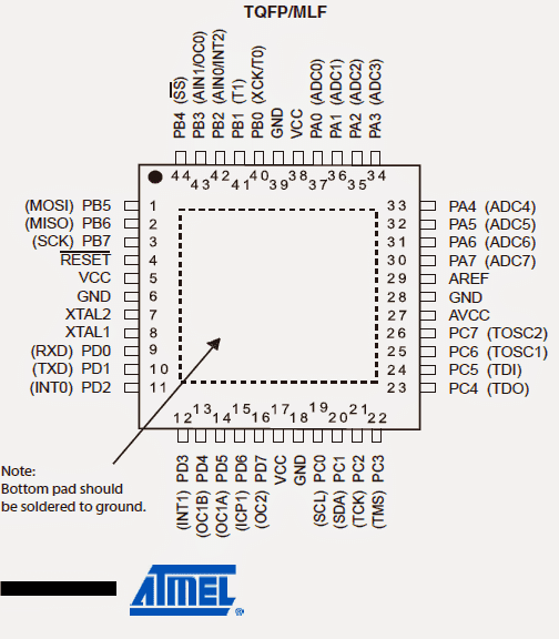
The various pinouts of this advanced MCU unit may be understood from the folowing data:

Vcc = It's the Supply voltage pin of the IC compatible with digital IC supply voltage (5V)

GND refers to "ground" should be connected to the negative rail of the supply.

Port A (PA7...PA0): Here port A facilitates in the form of analogue inputs for the A/D converters. This port may be also used as an 8-bit bi-directional Input/Output port, only when the A/D converter is excluded from being used.
Port pins are facilitated with in-built pull-up resistors (each bit being assigned).

The Port A buffered outputs also provide a well balanced and symmetrical drive characteristics inclusive of high sink and source capability.

When pins across PA0 and PA7 are assigned as inputs and are externally subjected to a logic low, they begin sourcing current as soon as the internal pull-up resistors get energized.

All the above discussed pinouts are tri-stated when the reset is triggered (even without the clocks being activated), tri-state refers to three types of conditions which the IC is able to produce: high, low, and non-responsive or open.

Port B (PB7...PB0): Basically, just like Port A, this Port also is an bi-directional 8 bit input/output port featured with internal pull-up resistors (configured for each bit). The drive characteristics assigned to to Port B buffered pins are equipped with both high sinking and sourcing attributes.

When used as inputs, these pins source current when these are puled low by the external circuit stage due to the internal pull-up resistors being activated. The Port B pins are also designated with a tri-state feature.

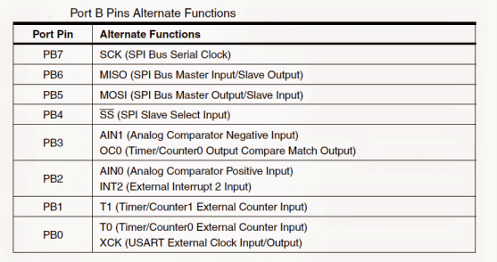
Apart from the above, Port B pins could be also used for implementing special features, as included in Atmega32, these are listed in the following table:
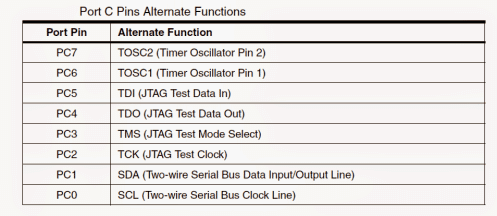
Port C (PC7...PC0): Port C pinouts also enjoy the various characteristics features enabled for the Port A and Port B.

However, apart from the identical features of port A and B, the internal pull-up resistor for Port C pins PC5(TDI), PC3(TMS) and PC2(TCK) all become activated even during a reset action in case when JTAG interface is toggled.

Additionally Port C also carries out the function of JTAG interface and other specified features of ATmega32 as shown in the below table:
 

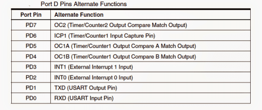
Port D (PD7..PD0): Again just like the above ports, the fundamental current sinking and sourcing characteristics of Port D is exactly the same.

However when used alternately these pins may be used for enforcing special ATmega32 functions which may be studied through the following table:
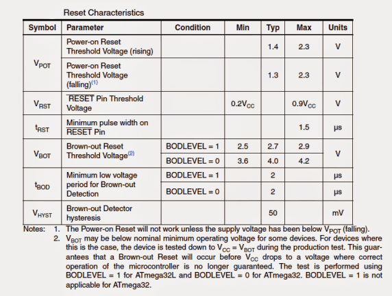
RESET: As the name suggests, the reset pinout may be used for resetting or forcing the IC to resume its functioning may be simply done by applying a low logic pulse here, however the minimum length of this pulse must not be less the specified pulse length of the IC. Anything shorter than this may not guarantee a reset action.

The following table indicates the minimum reset pulse length applicable:
XTAL1: May be used for latching on to a given frequency and for enabling a flawless frequency response across the input pin of the inverting amplifier and input of the internal clock producing circuit.

XTAL2: Just as above this may be configured across output pinout of the inverting oscillator amplifier

AREF: It refers to the analogue reference pinout assigned for the internal A/D converter stage
You'll also like:

  • arduinodisplayconnectionArduino Frequency Meter Using 16 x 2 Display
  • Receiver12312 2Wireless Servo Motor Control Using 2.4 GHz communication link
  • simulation2B1 1Transformerless AC Voltmeter Circuit Using Arduino
  • High Current Motor Control Circuit using Arduino

Filed Under: Arduino Projects Tagged With: ATmega32, Explained, Pinouts

About Swagatam

I am an electronics engineer and doing practical hands-on work from more than 15 years now. Building real circuits, testing them and also making PCB layouts by myself. I really love doing all these things like inventing something new, designing electronics and also helping other people like hobby guys who want to make their own cool circuits at home.

And that is the main reason why I started this website homemade-circuits.com, to share different types of circuit ideas..

If you are having any kind of doubt or question related to circuits then just write down your question in the comment box below, I am like always checking, so I guarantee I will reply you for sure!


Previous Post: « Programmable Automatic Starter Circuit for Diesel Water Pump
Next Post: Fishing YoYo Stop-Motion Switch Circuit with Indicator »

Reader Interactions

Questions & Answers

Total Posts: 1
Newest Oldest
shadab karnachi
December 1, 2014 • 12 years ago #27404

can 8 bit output be sent through atmega 16

Reply

Need Help? Please Leave a Comment! We value your input—Kindly keep it relevant to the above topic! Cancel reply

Your email address will not be published. Required fields are marked *

Primary Sidebar

My YouTube Channel

Circuit Simulator: Draw and Simulate Schematics

circuit simulator image


Categories

  • Arduino Projects (95)
  • Audio and Amplifier Projects (134)
  • Automation Projects (18)
  • Automobile Electronics (104)
  • Battery Charger Circuits (90)
  • Datasheets and Components (109)
  • Electronics Theory (151)
  • Energy from Magnets and Earth (43)
  • Games and Sports Projects (11)
  • Grid and 3-Phase (20)
  • Health related Projects (27)
  • Home Electrical Circuits (13)
  • Indicator Circuits (16)
  • Inverter Circuits (98)
  • Lamps and Lights (161)
  • Meters and Testers (72)
  • Mini Projects (28)
  • Motor Controller (68)
  • Oscillator Circuits (30)
  • Pets and Pests (15)
  • Power Supply Circuits (91)
  • Remote Control Circuits (50)
  • Security and Alarm (65)
  • Sensors and Detectors (107)
  • SMPS and Converters (46)
  • Solar Controller Circuits (62)
  • Temperature Controllers (44)
  • Timer and Delay Relay (51)
  • Voltage Control and Protection (44)
  • Water Controller (37)
  • Wireless Circuits (31)


Subscribe to get New Circuits in your Email


Other Links

  • Privacy Policy
  • Cookie Policy
  • Disclaimer
  • Copyright
  • Videos
  • Sitemap

People also Search

555 Circuits | 741 Circuits | LM324 Circuits | LM338 Circuits | 4017 Circuits | Ultrasonic Projects | SMPS Projects | Christmas Projects | MOSFETs | Radio Circuits | Laser Circuits | PIR Projects |


Recent Comments

  • Swagatam on Inverter Circuit with Feedback Control
  • Swagatam on Proximity Detector IC CS209A Pinouts – Datasheet Explained
  • PRAFUL WANDHARE on Proximity Detector IC CS209A Pinouts – Datasheet Explained
  • Swagatam on 220V Solid State Relay (SSR) Circuit using Triac and OptoCoupler
  • Stathis on 220V Solid State Relay (SSR) Circuit using Triac and OptoCoupler

Social Profiles

  • Twitter
  • YouTube
  • Instagram
  • Pinterest
  • My Facebook-Page
  • Stack Exchange
  • Linkedin

Calculators

  • ZVS Induction Heater + Tank Calculator Tool
  • Zener Diode Calculator
  • Wire Current and Thickness Calculator (Ampacity Calculator)
  • Voltage Divider Calculator
  • Transistor Base Resistor Calculator
  • Transistor Astable Multivibrator Calculator
  • TL431 Calculator
  • Solar Panel, Inverter, Battery Calculator
  • Ferrite Core Air Gap Calculator Tool
  • Parallel MOSFET Calculator Tool: How to Connect MOSFETs in Parallel Safely
  • LC Resonance Calculator for EV Battery Charger Circuits
  • LED String Series Resistor Calculator
  • PFC (Power Factor Correction) Calculator Tool: 3kW
  • Passive Power Factor Correction (PFC) Calculator
  • LM567 IC Calculator Tool
  • SMPS Flyback Boost Converter Calculator
  • Shunt Resistor Calculator for Ammeters
  • SCR and Triac Gate Resistor Calculator
  • Battery Back up Time Calculator
  • Boost Converter Calculator (Non-Isolated)
  • Bootstrap Capacitor Calculator
  • Buck Converter Calculator
  • Buck-Boost Converter Calculator
  • Capacitance Reactance Calculator
  • DCM Flyback Transformer & Wire Gauge Wire Size Calculator Tool
  • Filter Capacitor Calculator
  • IC 4047 Calculator (Frequency and PWM)
  • IC 4060 Calculator
  • IC 555 Astable Calculator
  • IC 555 Monostable Calculator
  • IC SG3525, SG3524 Calculator
  • Inductance Calculator
  • Induction Heater Inductor and Resonant Frequency Calculator
  • Induction Heater Work Coil Calculator
  • Inverter LC Filter Calculator
  • LC Resonance Calculator
  • LED Current Calculator
  • LM317, LM338, LM396 Calculator
  • NAND/NOT Gate RC Values Calculator
  • NOT, NAND Gate Frequency Calculator
  • Notch Filter Calculator Tool
  • Ohm’s Law Calculator
  • Phase Angle Phase Shift Calculator
  • Power Factor (PF) Calculator
  • RC Filter Calculator
  • Reactance Calculator
  • Sine Table Calculator for SPWM Arduino Code
  • Small Signal Transistor(BJT) and Diode Quick Datasheet
  • SMPS Calculator for Toroidal Ferrite Transformers
  • SMPS Flyback Transformer Calculator – Design by Target Duty Cycle
  • TL431 Calculator
  • Op-Amp Hysteresis Resistor Calculator

© 2026 · Swagatam Innovations