The Atmel AVR Atmega32 is a low power CMOS based microcontroller chip manufactured on the AVR advanced RISC architecture. It is featured for carrying out technologically powerful instructions within each of its clock cycles.
The chip is also equipped with the capability of achieving throughputs rated at 1MIPS per MHz enabling the system manager to enforce an efficient or optimal ratio of power consumption to processing speed.
Understanding the Pinout Functions
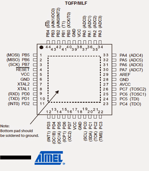
The various pinouts of this advanced MCU unit may be understood from the folowing data:
Vcc = It's the Supply voltage pin of the IC compatible with digital IC supply voltage (5V)
GND refers to "ground" should be connected to the negative rail of the supply.
Port A (PA7...PA0): Here port A facilitates in the form of analogue inputs for the A/D converters. This port may be also used as an 8-bit bi-directional Input/Output port, only when the A/D converter is excluded from being used.
Port pins are facilitated with in-built pull-up resistors (each bit being assigned).
The Port A buffered outputs also provide a well balanced and symmetrical drive characteristics inclusive of high sink and source capability.
When pins across PA0 and PA7 are assigned as inputs and are externally subjected to a logic low, they begin sourcing current as soon as the internal pull-up resistors get energized.
All the above discussed pinouts are tri-stated when the reset is triggered (even without the clocks being activated), tri-state refers to three types of conditions which the IC is able to produce: high, low, and non-responsive or open.
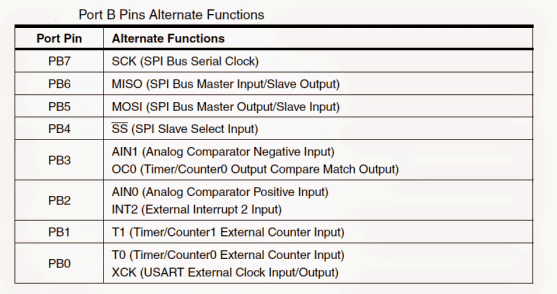
Port B (PB7...PB0): Basically, just like Port A, this Port also is an bi-directional 8 bit input/output port featured with internal pull-up resistors (configured for each bit). The drive characteristics assigned to to Port B buffered pins are equipped with both high sinking and sourcing attributes.
When used as inputs, these pins source current when these are puled low by the external circuit stage due to the internal pull-up resistors being activated. The Port B pins are also designated with a tri-state feature.
Apart from the above, Port B pins could be also used for implementing special features, as included in Atmega32, these are listed in the following table:
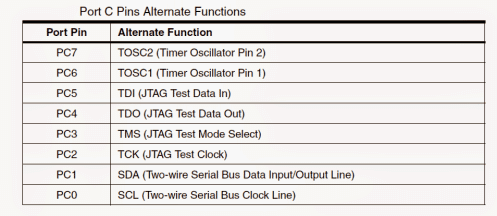
Port C (PC7...PC0): Port C pinouts also enjoy the various characteristics features enabled for the Port A and Port B.
However, apart from the identical features of port A and B, the internal pull-up resistor for Port C pins PC5(TDI), PC3(TMS) and PC2(TCK) all become activated even during a reset action in case when JTAG interface is toggled.
Additionally Port C also carries out the function of JTAG interface and other specified features of ATmega32 as shown in the below table:
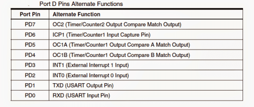
Port D (PD7..PD0): Again just like the above ports, the fundamental current sinking and sourcing characteristics of Port D is exactly the same.
However when used alternately these pins may be used for enforcing special ATmega32 functions which may be studied through the following table:
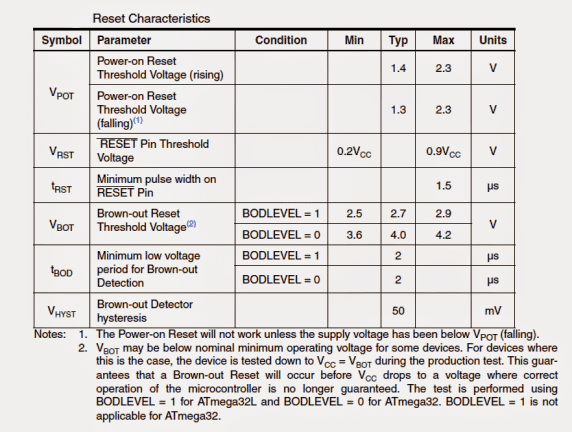
RESET: As the name suggests, the reset pinout may be used for resetting or forcing the IC to resume its functioning may be simply done by applying a low logic pulse here, however the minimum length of this pulse must not be less the specified pulse length of the IC. Anything shorter than this may not guarantee a reset action.
The following table indicates the minimum reset pulse length applicable:
XTAL1: May be used for latching on to a given frequency and for enabling a flawless frequency response across the input pin of the inverting amplifier and input of the internal clock producing circuit.
XTAL2: Just as above this may be configured across output pinout of the inverting oscillator amplifier
AREF: It refers to the analogue reference pinout assigned for the internal A/D converter stage


Comments (1)
can 8 bit output be sent through atmega 16