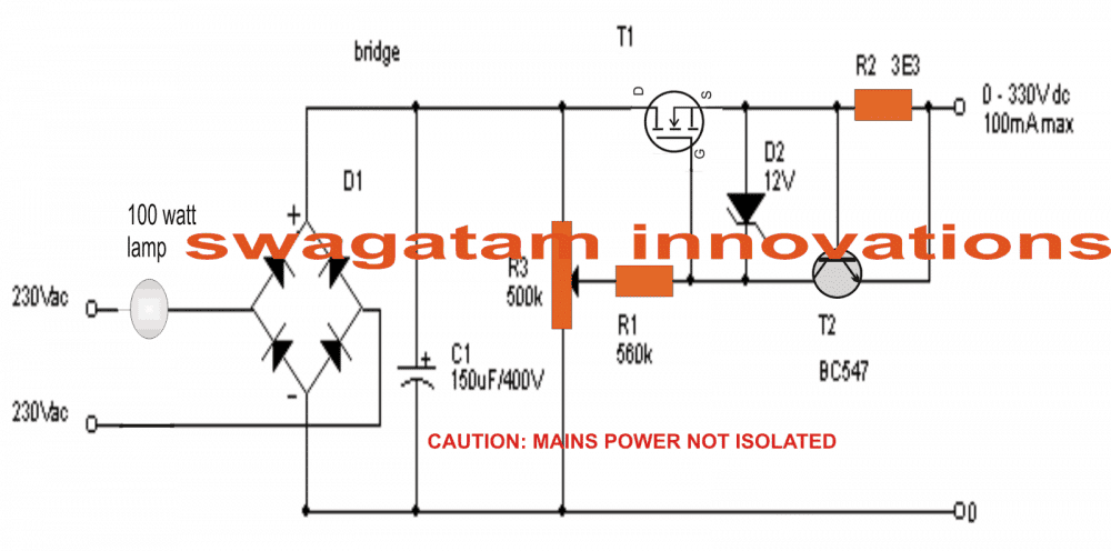
This simple MOSFET controlled transformerless power supply circuit can be used for delivering a continuously variable 0 to 300V DC output and a current control from 100 mA to 1 Amp.
To protect against my high voltage research projects from going up in smoke permanently, I developed an easy circuit which is able to render a variable voltage supply of 0 to 330 Volt.
But please be cautioned, the circuit is not isolated from mains potential, and therefore can inflict a lethal shock.
The supply is short-circuit proof: the current is restricted to approximately 100mA.
WARNING: ALL THE ABOVE CIRCUITS CARRY LETHAL MAINS VOLTAGE AND THEREFORE ARE EXTREMELY DANGEROUS. IT CAN KILL ANYBODY, IF TOUCHED ANYWHERE ON THE CIRCUIT IN POWERED CONDITION. OBSERVE APPROPRIATE PRECAUTIONS TO AVOID ANY MISHAP.
Circuit Operation
The design does not require a transformer, rather a 100 watt bulb is introduced at the input in order to provide ultimate safety in case of a short circuit or a component failure.
The mains voltage from after passing through the lamp is rectified with bridge D1 (1Amp / 500V) and C1.
T1 is configured as a source follower: the source of T1 complies with the voltage of the wiper of R3. D2 is insured to safeguard the gate of T1.
T2 and shunt resistor R2 establish the current limiter. Whenever the output current results in being excessive, T2 quickly discharges the gate of T1.
This stops the current from increasing any further. The value of R3 was basically identified experimentally; however it actually depends on the Hfe of T2 which means you may need to adjust the value of R2 appropriately.
Keep in mind T1 requires a large heatsink: in nastiest situation T1 would probably disperse 330V x 100mA = 33Watt!
You may try mosfets such as a BUZ 326 (400V/10.5Amp) or you may likewise use an IRF740 (400V/10Amp).
The output impedance of the power supply varies according to the beta of T1, therefore the bigger the MOSFET, the lesser the output impedance!
Circuit Diagram
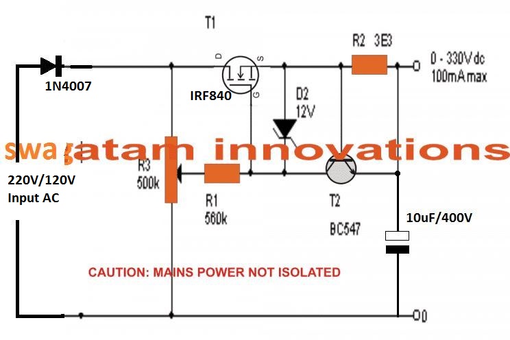
UPDATE:
The above design could be much simplified as indicated in the following diagram. The bridge rectifier has been eliminated which drastically reduces the stress level on the MOSFET.
However, the ripple generated due to a half wave rectification may be significantly higher.
The output 10uF filter capacitor helps to reduce this to some extent. The value of this capacitor could be increased to higher levels for improving the DC quality.
The input series lamp can be added, although this may not be required due to the presence of the current control stage in the design. However, for better safety a fuse may be added in series with the input line.
The output load specification must not exceed 100 ma
Video Proof:
This power supply can be used to obtain a regulated power output, variable right from zero to 300 volts maximum. All the devices should be mounted on heatsinks.
Working Principle
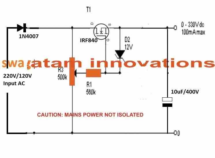
The circuit regulates the output voltage using an IRF840 MOSFET (T1) as the main regulating element.
The 500k potentiometer (R3) controls the gate voltage of the IRF840 thus varying the output voltage.
The output current is controlled via the current-sensing resistor R2. When the voltage drop across R2 exceeds the base-emitter voltage of the BC547 transistor (T2 typically 0.6V to 0.7V) then T2 turns ON and reduces the gate voltage of T1 limiting the current.
D2 (12V Zener diode) ensures that the voltage of the IRF840 between its gate and source does not exceed 12V.
Key Parameters
- Vout: Adjustable output voltage (0–300V DC)
- Iout: Maximum output current (A)
- R2: Current sensing resistor (ohms)
- R3: Potentiometer for voltage control (ohms)
- Vin: Input voltage (rectified 220V AC ≈ 310V DC)
Formulas
- Output Voltage Control
The gate voltage of T1 is determined by the setting of the 500k potentiometer (R3). The output voltage is approximately proportional to the gate voltage of T1.
Vout ≈ Vgs(T1) - Vds(on)
- Where:
- Vgs(T1) = Gate-to-source voltage of T1
- Vds(on) = Drain-to-source voltage when T1 conducts (small value around few volts)
- Current Limiting (Iout)
The current limiting is handled by the sensing resistor R2. The voltage drop across R2 is compared with the base-emitter voltage of T2 (Vbe approximately 0.6V–0.7V). When the voltage drop across R2 exceeds Vbe, T2 turns ON and reduces the gate voltage of T1, thereby limiting the current.
Iout = Vbe / R2
- Where:
- Iout = Maximum output current (A)
- Vbe = Base-emitter voltage of T2 (typically 0.6V–0.7V)
- R2 = Current sensing resistor (ohms)
- Power Dissipation in R2
The sensing resistor R2 must dissipate power proportional to the output current:
P(R2) = Iout2 * R2
- Where:
- P(R2) = Power dissipated in R2 (W)
Choose a resistor with a power rating higher than P(R2) for safe operation.
- MOSFET Power Dissipation
The IRF840 MOSFET dissipates power due to the voltage drop across it and the output current:
P(T1) = (Vin - Vout) * Iout
- Where:
- P(T1) = Power dissipated in T1 (W)
- Vin = Input voltage (DC, ≈310V for rectified 220V AC)
- Vout = Output voltage (adjustable)
- Iout = Output current (A)
Ensure T1 has adequate heat sinking to handle the calculated power dissipation.
Example Calculations
Let us Assume:
Vin = 310V DC peak rectified from 220V AC.
Vout = 300V DC
Iout = 0.5A (desired maximum current)
Vbe = 0.6V
Step 1: Calculate R2 (Current Sensing Resistor)
R2 = Vbe / Iout = 0.6 / 0.5 = 1.2 ohms
Step 2: Power Dissipation in R2
P(R2) = Iout2 * R2 = 0.52 * 1.2 = 0.3W
Choose a resistor with at least a 0.5W rating for safety.
Step 3: Power Dissipation in T1 (IRF840)
At maximum output:
P(T1) = (Vin - Vout) * Iout
= (310 - 300) * 0.5
= 10 * 0.5 = 5W
At lower output voltages the power dissipation in T1 will increase so choose the heat sink to handle the worst-case scenario.
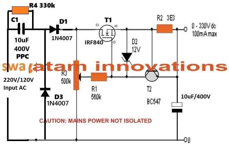
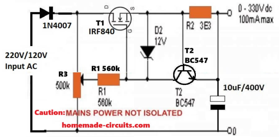
A Failproof 300V Variable Power Supply Design
To make the above 300V adjustable power supply completely safe and failproof, you can modify it by adding an input current limiting capacitor, as shown in the following diagram.
However, please remember that the circuit is safe and failproof only for the MOSFET, but it still carries a floating 300V AC, which can be lethal for any human if the circuit is touched in open and powered condition.
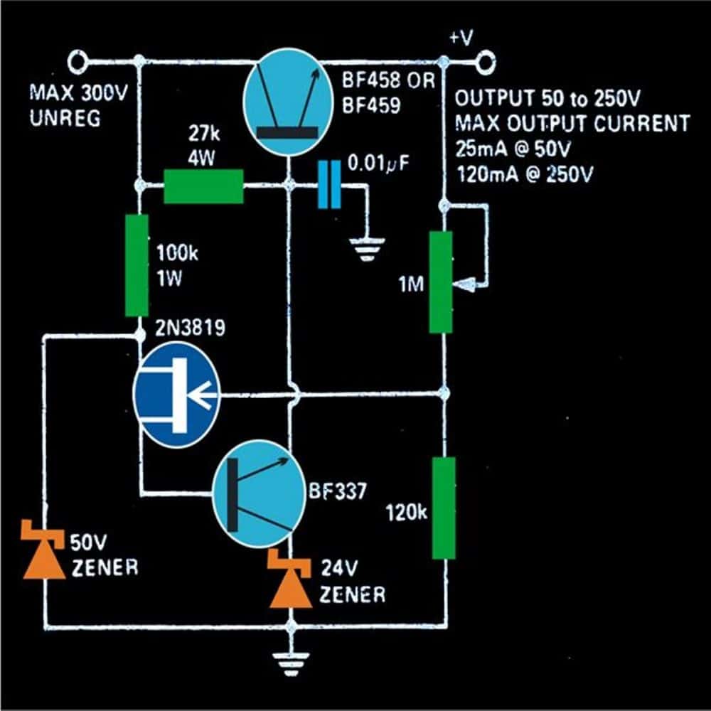
Using a Combination of BJT and Mosfets
Circuit Operation
The next transformerless 0-300V variable power supply circuit diagram can be understood with the following points:
As can be seen in the figure, a high voltage transistor BF458 is used as the main load handling device.
Its base bias is controlled by another high voltage transistor BF337 whose emitter is clamped to a stable 24 volts.
An FET is used for selecting the base current of the transistor BF337 via a pot of 1M.
This setting adjusts the base current for the BF337 which in turn restricts the main transistor BF458s voltage and current flow to the output.
The input to the circuit may be derived directly from the mains AC after proper rectification and filtration using a bridge network and a 10u/400V capacitor.
The entire circuit is extremely dangerous to touch, due care should be maintained while making and testing this circuit.
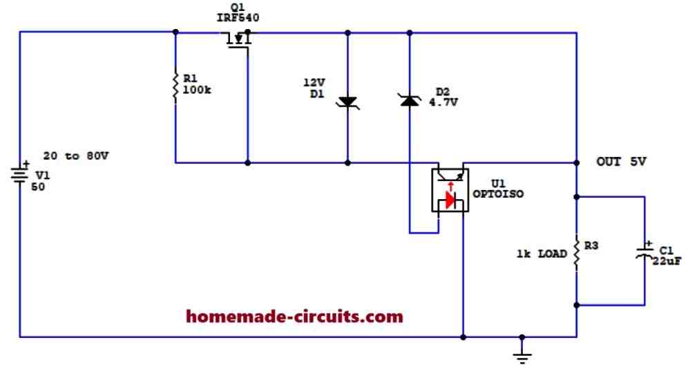
Converting 80V DC to 5V DC Stabilized Output
The above explained 300V MOSFET regulator circuit was successfully modified by Mr. Luigi to convert a varying input between 20V and 80V DC into a stabilized 5V DC output, using an opto-coupler feedback, as shown in the following figure. I am grateful to Mr. Luigi for contributing this design to this website.

Questions & Answers
Please I am a beginner in circuits and find it some how difficult to read schematics.I would please like to know where the emitter of the transistor BC 547 is connected to in the circuit above and possible the connection between the R2, the 12V diode and the MOSFET.Thank you .Greetings from Ghana
Hi, please check this diagram, is it OK now:
Emitter of BC547 is connected to 10uF capacitor and the output…
Sayın Swagatam cevabınız için çok teşekkür ederim.
You are most welcome Mehmet!!
Hay its me again, very good circuit, used it for testing inverters. Works very well. Thank you for your web site and your knowledge. You are the bomb.
Hey Arthur, thanks for your candid feedback, I am glad you found the above circuit helpful…please keep up the good work…
Good evening Swagatam,
I’m collecting ideas to build a tube-tester (valve-tester?) out of recycled parts and this article is very useful to me.
By the way, thanks a lot in advance for sharing your knowledge.
I will use a transformer and protect it with a fuse, so we can keep this in mind. This schematic will be the part I want to build to provide the anode voltage to the tube, so let’s treat it as a module of the final project.
What I want to achieve is getting a voltage with a limited swing, about 150V to 300V DC, but since the heaviest tube I want to test can pull about 150mA, I need to change some parts and this is why I’m writing here.
First of all the R sense should let 200mA to pass, so, if we consider Vbe of T2 like 0,6V, R=V/I=3Ohm, so a little bit different (I have to make some series o parallel to obtain the right value…), but what about T2 type? What can I use instead of BC547 to handle such current without burning?
Second modification: I think, for T1, IRF840 can be a better choice for me, right?
Third modification: since I don’t need to go as low as 0V, I think I can use a 250K pot instead of 500K, then a series of zener diodes (with K toward the pot) with the sum of Vz equal to my minimum voltage required, right? Do you think 250K is the right value, or do you suggest a different one? I think R1 should be left as is…
The output will go to the anode of the tube and a digital Voltmeter panel mounted, so that I can vary the voltage measuring it and, together with the readings of the other instruments, I can calculate the tube constants.
Since I want to simplify the design, I think I will connect the anode and g2 together (for the pentode types) and measure the plate current placing a 1Ohm resistor between the cathode and ground, so the voltage across it will equal the current and I’ll be able to use a Voltmeter in parallel, for a better precision.
I have so may other things to ask, but they are about other parts of the tester, so I’ll do it somewhere else.
Thank you very much in advance, kind regards,
Alex
Thank you Alex,
If you are using a transformer then the second circuit would be quite suitable. You can connect the transformer AC directly at the input of the circuit.
The value of the pot actually does not matter, anything above 100k would work well, because only the ratio of the pot resistance is what determines the output voltage.
The BC547 does not handle the output current, it handles only the gate current dropped by the 560k resistor which is almost negligible.
The MOSFET can be IRF840 yes, as shown in the diagram.
Please let me know if you face any issues with the circuit. All the best to you…
Hi dear Swagatam;dizx))
I had sent my queston under the following article
https://www.homemade-circuits.com/prevent-amplifier-fuse-from-blowing-during-power-switch-on/#comments
and you have avised this page to share it.
As a result; I test my TV 220AC 160W with the 100W serial bulb and the bulb blinks but not regular for instant it blinks 5 times long period then 3 times short period however if change the bulb with a 15W then this time I see the regular blinks it blinks constantly in every second. And finally I use 14 uF capacitor as the serial then I see about 20 V in the serial capacitor but power card main capacitor has the initial voltage about 400V. So I need your comment for the situation
Thank you Suat,
You must check the voltage across the load, so if the main capacitor is the load and is showing 400V, then it is fine, but how is the TV behaving? Is it working?
Hi Swagatam, first of all I am sorry since my keyboard is defective and not able to print the letters d,i,z,x so I need to copy and paste and then forgot to erase the letters from the above message. If the all pcbs (power board – main board and T-Con) are connected together I see about 400V but If I check only single the power board I see about 298V and however at this time I check the power board while 5V and standby are short (There is no remote control and no any on/off switch on the TV case) then I see again about 400V. And also there were sound and no image since the front black glass screen was broken / crack.
Hi Suat,
So you mean to say the 14uF capacitor is giving 298V to the TV?
Yes, it will because it will pass the full input AC to the load at around 1 amp current.
GLAD TO ANNOUNCE THAT I HAVE BUILT THE CIRCUIT AND IT WORKED OUT VERY WELL. AT FIRST I WAS THINKING THE BC547 WILL FLASH BECAUSE I LOOKED AND DID NOT SEE ANY BIASING RESISTOR ATTACHED TO ITS BASE AND THE EMITTER IS NOT CONNECTED TO THE GROUND. I TESTED IT WITH 1OK, 1/2W AS LOAD AND WAS ABLE TO GET UP TO GET UP TO 20mA AT ABOUT 160V BEFORE IT STARTED SMOKING. I ALSO TESTED WITH 10 OHM, 5W RESISTOR AND WAS ABLE TO GET UP TO 160mA. ALTHOUGH THE OUPUT VOLTAGE WAS NEGLIGIBLE DUE TO THE FACT THAT 10 OHM RESISTOR WAS TO SMALL A VALUE AND THUS PREVENTING THE FILTERING CAPACITOR FROM BEING CHARGED. I LATER DID THE TRANSFORMER BASED FASHION AND IT ALSO WORKED FINE. ENGR. SWAGATAM, I AM VERY GRATEFUL FOR THIS YOUR AMAZING PLATFORM.
Thank you Mosses, I am glad it worked successfully for you…
Thanks for the nice work. Sir have you tested the circuit on full load or anything close to 90mA. I fear that bc547 might get too hot. I intend to make make this circuit to handle 200mA but I plan to use bc337. Is that ok or should I use 2n2222a instead.
Hello Moses, The load current is handled by the MOSFET, not by the BC547 transistor, so the BC547 is safe, and will not burn at any given output current. You can use any 50V 100mA NPN BJT in place of the BC547.
Ok thank you very much
You are welcome Moses.
Hi Swagatam,thank you for this circuit. Please, is it possible to use variable transformer (input 220VAC, output 0-300VAC) to control output DC voltage by controling AC output using this circuit? I need a variable power supply 0-350VDC also variable current supply 0-5A DC. This circuit is only for voltage DC output I understand but I need also a current regulated if there is any idea. Thank you!
Hi Bursach,
Yes, you can use the above circuit in conjunction with a variable AC output from the transformer. You can adjust the current by changing the values of R2 resistor…
Thank you!
I have one query on transformer less power supply.
Actually I’m going to design one power supply which will be transformer less.
I tried for many topologies. That was not sufficient to provide me 5V, 500mA from bridge rectifier output 330V. Capacitor and Resistor dropper having issue with current it can deliver max. 120mA.
If anyone have suggestion on any particular circuit, please suggest me. with schematic also mentioned output current.
You can try the last circuit with an opto coupler.
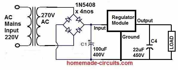
Make sure to replace the MOSFET with IRF840, and feed the 220V input AC through a 10uF/400V capacitor and a bridge rectifier (using 1N5408 diodes)
me again! Mr Swagatham! can you give me a formula to rotate the coil to have an output 220 V AC 110 V AC with step-down transformer
Fastra, you do not any formula or circuit if you are using a step-down transformer, you just need to connect the 220V side of the transformer to the 220V AC input and then get 110V AC from the other side of the transformer.
bonjour swagatam ! J’ai une imprimante laser jet 110v AC mais dans mon pays nous utilisons du 220v ac, pouvez-vous m’aider avec un schéma 220v ac convertir 110v ac, car le prix du transformateur abaisseur est très cher dans notre pays ! Merci pour votre aide, que Dieu vous bénisse, votre travail et votre famille !
Thank you Fastra, i can understand your problem, however there’s no easy circuit to convert a 220V AC to 110V AC, unless a transformer is involved.
An SMPS can be used, but that will be far more expensive than an ordinary iron core transformer version….and an SMPS will also require a huge lot of calculations.
merci beaucoup pour votre aide et information
Hello Swagatam! Is this schematic 0 to 300v adjustable suitable for me, for the printer 110v AC 300w hp lasert jet
Hello Fastra,
Sorry, no, the above design is not suitable for your application, because the above power supply is suitable only for DC loads.
I tried this circuit to reduce the voltage of a 48V photovoltaic system, max input voltage 75V. I needed a stable 5V voltage to power a pic MCU which reads the panel voltage and sends via isolated serial.
It works well, I used an optocoupler to stabilize the voltage. If you are interested, I can send you the diagram which is very simple.
Thank you Luigi, for trying this circuit for your specific application, yes I would be certainly interested to see the schematic.
Please send it to my following email ID:
homemadecircuits
@ gmail.com
I have had to put two of these in series. There is a parallel resistor load a voltage divider and circuitry at the first -150 VDC node then another 0D3 and more circuitry to feed at -300 VDC. The 0D3 can NOT handle more than 40mA continuous load after it starts. It’s not supposed to anyway, but a lot cheating went on. With voltage divider off -645 VDC they run at 323 VDC +/- 6%. I also tied in the other -323 into the second regulator. I tossed in some 1N4007s too just to keep them to themselves. And yes those too look like they are in backwards because of the positive ground and the negative voltage supply. Hopefully those two -150 volt outputs will equal a stable -300. I also put the Zener diodes up close to the MOSFETs to keep them at more constant temperature. The Zeners were drifting with temperature changes.
That sounds good! I hope you have used separate bridge rectifiers at the input sides, for the two -150V modules. This is important to ensure both the modules are completely isolated from one another.
I found out I actually need to run two of these in series from a voltage divider upstream that outputs 2 x -323 VDC but it can vary from between -303 and -343 VDC with the mains voltage. Will the two -150 VDC outputs sum to make a -300 VDC output in the second regulator or do I set the first one for -150 and the second one for -300 VDC out? I also want to put some diodes in between the two units to keep everything separate with no DC feeding back from the second regulator to the first or is that a waste of parts? I tried some DIY SMPS regulators. WAY TOO NOISY! I had pretty clean DC coming into the SMPS regulators but with the SMPS regulators switching it put lots of high frequency noise into everything, especially with the two of them! They sync’ed up together and it was awful.
I think it’s better to set the first one for -150 VDC and the second one for -300 VDC out. You can put diodes across the outputs of the two units to keep everything separate and avoid DC feedbacks.
There’s zener diode in the above circuit which can become a source of noise, so i think a 100uF/25V capacitor could be connected parallel to this zener diode to filter out the noise.
Additionally you can also put a high value capacitor across the outputs of each regulator circuit for further noise suppression.
On further inspection I need two of these set for -150 VDC, and the negative voltage IN comes off a 25K/25K voltage divider from a filtered -645 volt supply node so that gives me -323 volts that could vary between -302 and -343 volts, as per the unit’s specs and the mains voltage. If I tie across ONE -150 VDC output I should get -150 volts regulated and if I tie in across BOTH (two) -150 VDC outputs I should get -300 volts regulated, correct? I need regulated -150 and regulated -300 regulated voltages. I have some other PSUs & some bread boards. If I strap the Lambda and the Japanese PSU together with diodes for safety that should give me a good -350 VDC @ 300 or so mA. I have tube power transformers around too! One would ALMOST work for the damaged transformer in my Nobatron 600B, but it’s 16 mm too tall to fit. : -(
Yes, that’s correct, you can connect the outputs of the two -150V supplies in series to get two -150V individually, and also one -300V DC output.
If I wanted to make this into a NEGATIVE 300 volt regulator would using a P channel MOSFET and a PNP BJT work? It’s just a pass tube bias supply, with reference sense & send regulation circuitry and it SHOULD only draw 40mA-60 mA. I’d think the Zener diode may have to be reversed too. I’d like those 0D3 tubes to go away.
Yes, you can convert the above shown design into a -300V regulated DC supply generator by using P-channel MOSFET and PNP BJT.
The P-channel mosfet can be also replaced with an equivalent PNP BJT.
The bridge rectifier polarity will also need to be changed for this application.
Yes, the zener orientation will also need to be reversed.
I started looking for P channel MOSFETS and PNP BJTs and THANK YOU THANK YOU so very much for confirming that theory! I shall have to make TWO that run at 150 volts each! I am coming off of a wacky isolated center tapped winding on a “main transformer” that is more or less wired up backwards with a 5R4 rectifier tube with the center tap being positive, relative with all of the filter caps being wired in reverse polarity. The two 0D3 tubes draw 100 mA EACH to start and these stupid designers HOPED they would start before they overheated an undersized $400+ 1170 VCT transformer. It’s just for voltage regulation (6BQ6 sweep tube pentode), reference/regulation voltage for the pass tube bias (5651 & a 6SL7), the feedback, and two regulated bias 0- -150 VDC voltage bias supply. There are two other windings in the transformer: A 240 VAC with no center tap @ ~ 75 mA for the 7 pass tube screen grids, and the 5R4 rectifier’s 5 volt 2 amp filament supply. Switching the unit off and on quickly would have all 7 5881 pass tubes running preheated with NO bias until the 0D3s restart. That jumps the screen current way up and that often fries that 240 VAC transformer winding and often cooks a selenium rectifier too. I already have -725 that is stepped down to -475 VDC post filter caps & some dropping resistors. There is my negative DC voltage supply for this regulator. Eliminating those two 0D3 VR tubes eliminates that 200mA starting current surge load. I may even replace the 5R4 with some 1N5408 diodes & shunt caps in a tube socket. The pass tube plates run off of a 970-0-970 or 1940 VCT transformer, and that filters through a gigantic choke & 3 450 VDC 82uF caps run in series with an old 50 watt 5K x 3 ohm Ward Leonard “voltage divider”. Reading about Ward Leonard (the man and the company) was very educational. I am adding an ON DELAY that activates and keeps the pass tubes OFF for 10 minutes if there is a short duration power outage or if some idiot toggles the unit off and on in quick succession. I can fit these regulator in tube sockets and just plug them into the 0D3 sockets and not worry about those 0D3s not lighting up in time. THANKS AGAIN! I am just an old stupid disabled electrician! I did PLC, relay logic, motor controls, instrumentation,4-20 mA, fire alarm, smart buildings, POI, etc. THANKS AGAIN! I loved working with the Indian electrical engineers. The white American engineers tended to be really lazy and very sloppy. I worked with some very good Pakistanis & an exceptional Englishman too, that were excellent engineers. The American EEs would keep adding stuff and forget to increase the load calculations. That’s just lazy and sloppy, and I have to do all of the calculations out in the field and send the plans back in. .
Thank you so much for the detailed explanation, it is indeed great to hear about tubes in this era of microchips.
Do let us know how the 300V controller circuit using transistors works for your application.
And feel free to ask or share any further questions or doubts you may have.
I have an old tube regulated PSU that uses two 0D3 VR tubes, which will regulate around 475 volts DC to 300 VDC with a constant load of around 35mA. Will this be stable @ 300 volts? Worst case it can surge to 60 mA or so.
The above circuit is extremely stable with its set output voltage.
Dear Swagatham, This is something that I been working on for a couple of days blowing a hell lot of Mosfets and Pots.
I have a couple of issues , that I hope you can help with.
1) Can I use the first circuit without the last current limitting section after the zenner diode with a 90 v dc input to get full current from the transformer ? (5 Amps) ( I can use really heavy heatsink for the mosfet).
1) When I connect only source to the positive of the 90 volt supply. I get voltage at the drain and gate too. Is that normal ? (Drain and gate not connected at all to anything). Since full 90 v is seen at the gate ,it develops a 10 to 80 ohm resistance between source and gate almost like a permanent short. it won’t work later.
2) A s source follower, can we get 0-90 v control since the gate voltage is clipped at the zenner diode voltage (12v or below the 20 v Vgs).
3) is the output current limited by the wattage of zenner diode ?
pls comment when you get time. thanks in advance.
Dear Suresh,
Here are the answers to your questions:
1) Yes you can use the first without current limit, however the second diagram is more efficient so i would suggest you the second diagram. Please check the modified version of the second diagram in the following figure:
The source is not supposed to be connected to a supply because the source is the output not the input. The supply input must be connected to the drain.
2) From a MOSFET source follower you wwill get from 0 to 85V, since 5V might get dropped by the MOSFET. 12V zener diode between gate and source will not impact the source voltage, it will impact if the zener diode is connected across the gate and the ground line.
3) The output is limited to the MOSFET current handling capacity, not the zener wattage.
Hallo!
Thanks for information about transformerless power supplies!
Is it reasonable to use your “0-300V Adjustable MOSFET Transformerless Power Supply Circuit” for high power applications?
For example I am interested in using this kind of power supply with up to 5KW regulated load with current of 13A and more.
So, is your power supply a good idea for abovementioned example?
I think that there will be a lot of power needed to be dissipated with super-extra large heat-sinks which could be as big or bigger than a transformer.
Am I right?
Sorry I am just a beginner in this field
Best wishes from Latvia
Rahims.
Hello,
You are right, this MOSFET power supply is not suitable for high power applications, since it will dissipate huge amounts of power and will require enormously big heatsink.
Thank you very much!!