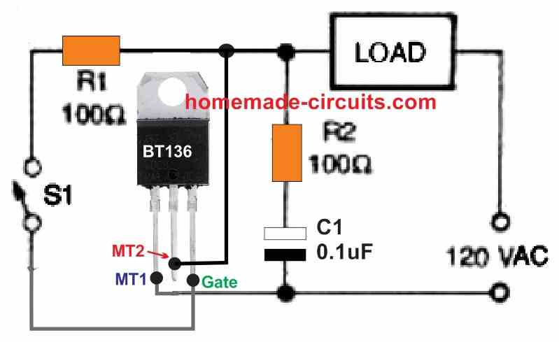
Using a set of latch/reset networks it becomes possible to allow a logic to move in a forward sequence, switching ON a given set of outputs HIGH, in response to an alternating input clock. And once the max limit is reached, the input clocks begin shutting down or withdrawing the sequence in the opposite order.
Thus, the up down sequence is controlled through a single oscillating input clock signal.
The process can also be explained as follow:
In response to an applied switching clock the circuit begins adding HIGH logics at the outputs in an incrementing sequence and once the maximum limit is reached, it begins subtracting the HIGH from the output by rendering them LOW in the opposite sequence, in response to the applied clock signals.
Here only 4 outputs are shown since the IC 4043 has only 4 pairs of set/reset latches, nonetheless the number could be possibly increased by cascading the IC 4017 and by adding another 4043 IC with the existing one. This would allow us to get 8 numbers sequencing set/reset or 8 pairs of up/down outputs.
Application
This circuit can be very useful for controlling a given parameter such that any further increase of the parameter is inhibited as soon as the maximum limit is exceeded, and conversely the process is restored and initiated when the limit comes back within the range.
For example it can be applied in small elevators to allow only 3 people to get inside the lift, once this limit exceeds, the elevator is inhibited from starting, but once the limit is restored the elevator is allowed to move.

How this UP/DOWN sequencer Works
This circuit was originally created to start up power supplies in sequence and subsequently switch them off for a second time in the opposite sequence. This feature can be often useful for tinkering with equipment and circuits where power needs to be employed and taken out in a specific order.
The main section of the circuit is the work horse IC 4017 CMOS decade counter. Outputs Q1 to Q4 are accustomed to establish latches serially in the order of 1-2-3-4, after which the counting is stopped. Pressing switch S1 enables the counting to carry on, and now the counter outputs Q5 to Q8 are applied to reset the latches in the opposite sequence, meaning in the order 4-3-2-1. The last output, Q9, is utilized to stop the counter.
As soon as power is switched ON, C2 and R2 at first render the counter in the reset position. Once the power supply voltage becomes steady, the reset signal eventually goes low allowing the 4017 to begin the counting at the 1-Hz clock signal which is acquired through an oscillator composed of IC1d, R3 and C3.
The output pins of IC 4017 are triggered in succession with every rising edge of the clock pulse.However as the following clock pulse arrives the last output shuts down.
The latches in the quad RS-latch type 4043 make it possible for the outputs to remain activated. IC2 ceases counting at Q4 because of IC1b which removes the clock-enable signal at pin 13 through IC1a.
In order to permit the 4017 to carry on counting and therefore switch off the outputs, S1 needs to be pressed, which reestablishes the clock-enable at pin 13.
Counter outputs Q5 to Q8 are attached to the reset inputs of the latches, so as IC2 sequence moves down, the latches get reset in the reverse direction. The counting process is eventually ceased at Q9 by IC lc, that yet again takes away the clock-enable signal.
High value, low current pull-up resistors (R4-R7) are employed on the latch ‘reset' inputs in order to avoid undefined start off situations.
Parts List
Resistors (All resistors are 1/4 wat 5%)
R1 = 4K7
R3 = 4M7
R2, R4, R5, R6, R7 = 1M
Capacitors
C1, C4, C5 = 0.1uF/ceramic
C2 = 22uF/25V
C3 = 1uF/25V
Integrated Circuits
IC 4017 = 1no
IC 4043 = 1no
IC 4093 = 1no
S1 = push to ON switch


Comments
Hi Swagatam
I want to configure the circuit as follows.
I used two push button ‘Up’ and ‘Down’ to energize and deenergize 6 relays.
when i push ‘up’ button fist time need first output(one relay energize). Then i push ‘up’ button 2nd time need output 1st with 2nd (two relays energize). then i push ‘up’ button 3rd time need output 1st and 2nd and 3rd(three relays energize). it will go to until 6th. then its come down. if i press ‘up’ button 1 time or 2 time or 3 time………….. after that come back from the place i stopped.
please help with circuit
best regards
Anuradha
Hi Anuradha, 6 sequence up/down looks difficult, I do not have this design idea with me at this moment…only 4 sequences is feasible using the above explained circuit.
Ok swagatam, send me 4 sequence system.
much appreciate your replay and help
best regards, Anuradha
Hi Anuradha, the 4 sequence option is provided in the above article, you just have to add relay driver stages to the 4043 IC output pins.
For the relay driver circuit you can refer to the following article
Transistor Relay Driver Circuit with Formula and Calculations:
Sir please i am trying to design a project for my exams….i am pleading for you to help me with some modifications please…..can i email you the sample projects.
Sincerely nkwenti
NKwenti, you can explain it here, I will try to help!