A buffer stage basically a reinforced intermediate stage which allows the input current to reach the output without getting affected by the output loading.
In this post I will try to explain what digital buffers are, and we will be taking a look at its definition, symbol, truth table, double inversion using logic “NOT” gate, digital buffer fan out fan in, tri-state buffer, tri state buffer switch equivalent, Active “HIGH” tri-state buffer, Active “HIGH” inverting tri-state buffer, Active “LOW” state tri-state buffer, Active “LOW” inverting Tri-state buffer, tri-state buffer control, tri-state buffer data bus control and finally we will take an overview on commonly available digital buffer and tri state buffer ICs.
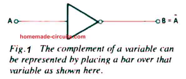
In one of the previous posts I have explained about logic “NOT” gate which is also called digital inverter. In a NOT gate output is always complementary to input.
So, if the input is “HIGH” the output turns “LOW”, if the input is “LOW” the output turns “HIGH”, so this is called as inverter.
There could be a situation where the output needs to be separated or isolated from the input, or in cases where the input may be quite weak and needs to drive loads requiring higher current without inverting polarity of the signal using a relay, or transistor etc. In such situations digital buffers become useful and are effectively applied as buffers between the signal source and the actual load driver stage.
Such logic gates which can deliver signal output same as input and act as intermediate buffer stage is called digital buffer.
A digital buffer does not perform any inversion of the fed signal and it is not a "decision making" device either, like logic “NOT” gate, but gives out the same output as input.
Illustration of Digital Buffer:
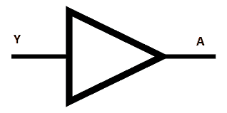
The above symbol is similar to logic “NOT” gate without the “o” at the tip of the triangle, which means that it does not perform any inversion.
The Boolean equation for the digital buffer is Y = A.
“Y” is the input and “A” output.
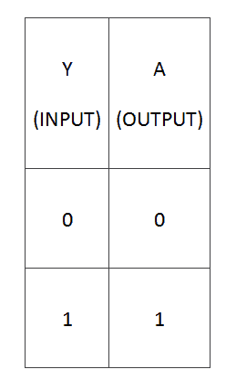
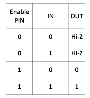
Truth table:
Double Inversion using logic “NOT” gates:
A digital buffer can be constructed using two logic “NOT” gates in the following manner:
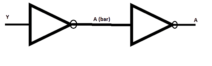
The input signal is first inverted by the first NOT gate on left hand side and the inverted signal is then further inverted by the next “NOT” gate on the right hand side, which makes the output same as input.
Why Digital Buffers are Used
Now you might be scratching your head why the digital buffer even exist, it does not do any operation like other logic gates, we could just throw the digital buffer out of a circuit and connect a piece of wire…….correct? Well not really.
Here is the answer: A logic gate does not require a high current to perform any operations. It just requires a voltage level (5V or 0V) at low current is enough.
All types of logic gates primarily support a built in amplifier so that the output is not dependent on input signals. If we cascade two logic “NOT” gates in series we get same signal polarity as input at the output pin but, with relatively higher current. In other words digital buffer works like a digital amplifier.
A digital buffer can be used as an isolation stage between signal generator stages and driver stages; also it helps prevent impedance affecting one circuit from another.
A digital buffer can provide higher current capability which can be used for driving switching transistors more efficiently.
The digital buffer provides higher amplification which is also called “fan-out” capability.
Digital buffer fan-out capability:
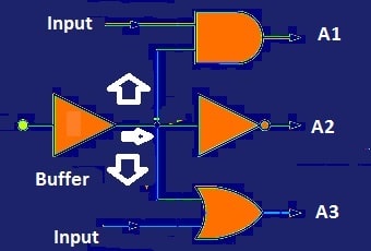
FAN-OUT: The fan-out can be defined as the number of logic gates or digital ICs that can be driven in parallel by a digital buffer (or any digital ICs).
A typical digital buffer has fan-out of 10, which means the digital buffer can drive 10 digital ICs in parallel.
FAN-IN: The fan-in is the number of digital inputs that can be accepted by the digital logic gate or digital IC.
In the above schematic the digital buffer has fan-in of 1, which means one input. A ‘2-input’ logic “AND” gate has fan-in of two and so on.
From the above schematic a buffer is connected to the 3 inputs of three different logic gates.
If we just connect a piece of wire in the place of the buffer in the above circuit, the input signal might not be with sufficient current and causes voltage to drop across gates and might not even recognize the signal.
So in conclusion a digital buffer is used for amplifying a digital signal with higher current output.
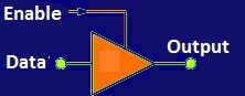
Tri-state Buffer
Now we know what a digital buffer does and why it exists in electronic circuits. These buffers have two states “HIGH” and “LOW”. There is another type of buffer called “Tri-state buffer”.
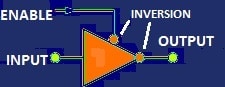
This buffer has an additional pin called “Enable pin”. Using the enable pin we can connect or disconnect the output from input electronically.
Like a normal buffer, it works as digital amplifier and gives output signal same as the input signal, the only difference is that the output can be electronically connected and disconnected by the enable pin.
So a third state is introduced, in this the output is neither “HIGH” nor “LOW” but an open circuit state or high impedance at the output and will not respond to the input signals. This state is referred as “HIGH-Z” or “HI-Z”.
The above is the equivalent circuit of the tri-state buffer. The enable pin can connect or disconnect the output from the input.
There are four types of Tri-state buffer:
• Active “HIGH” Tri-state buffer
• Active “LOW” Tri-state buffer
• Active “HIGH” Inverting Tri-state buffer
• Active “LOW” Inverting Tri-state buffer
Let’s look each of them sequentially.
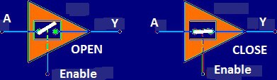
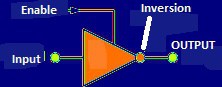
Active “HIGH” tri-state buffer
In the Active “HIGH” tri-state buffer (for example: 74LS241) the output pin gets connected to input pin when we apply “HIGH” or “1” or positive signal at the enable pin.
If we apply “LOW” or “0” or negative signal to the enable pin, the output gets disconnected from input and goes to “HI-Z” state where the output will not respond to input and output will be in open circuit state.
Active “LOW” tri-state buffer
Here the output will be connected to input when we apply “LOW” or “0” or negative signal at the enable pin.
If we apply “HIGH” or “1” or positive signal to enable pin, the output gets disconnected from input and output will be in “HI-Z” state / open circuit state.

Truth Table:
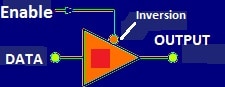
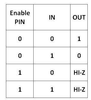
Active “HIGH” Inverting Tri-state Buffer
In active “HIGH” inverting Tri-state buffer (example: 74LS240), the gate act as logic “NOT” gate but, with the enable pin.
If we apply “HIGH” or “1” or positive signal at the enable input the gate gets activated and act like a regular logic “NOT” gate where its output is inversion / complementary of input.
If we apply “LOW” or “0” or negative signal to the enable pin, the output will be in “HI-Z” or open circuit state.
Truth table:
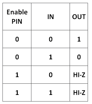
Active “LOW” Inverting Tri-state buffer:
In active “LOW” Inverting Tri-state buffer, the gate acts as logic “NOT” gate but, with enable pin.
If we apply “LOW” or “0” or negative signal to enable pin, the gate activates and work like regular logic “NOT” gate.
If we apply “HIGH” or “1” or positive signal to enable pin, the output pin will be in “HI-Z” state / open circuit state.
Truth Table:
Tri-state Buffer Control:
From the above we saw that a buffer can provide digital amplification and tri-state buffers can completely disconnect its output from input and give open circuit state.
In this section I have explained about the application of the tri-state buffer and how it is used in digital circuits for managing data communication efficiently.
In digital circuits we can find a data bus / wires carrying data, they carry all kinds of data in a single bus to reduce wiring congestion / reduce PCB traces and also reducing manufacturing cost.
At the each end of the bus, multiple logic devices, microprocessors and microcontrollers are connected which tries to communicate each other simultaneously which create something called contention.
Contention occurs in a circuit when some devices in a bus drives “HIGH” and some devices drives “LOW” simultaneously which causes short circuit and causes damage in a circuit.
Tri-state buffer can avoid such contention and properly send and receive data over a bus.
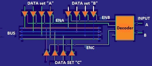
The tri-state buffer is used to isolate logic devices, microprocessors and microcontrollers from one another in a data bus. A decoder will allows only one set of tri-state buffers to pass data through the bus.
Say if the data set “A” is connected to a microcontroller, data set “B” to a microprocessor and data set “C” to some logic circuits.
In the above schematic all the buffers are active high tri-state buffer.
When the decoder sets the ENA “HIGH” the data set “A” is enabled, now the microcontroller can send data through the bus.
Rest of the two data sets “B” and “C” are in “HI-Z” or very high impedance state which electrically isolates the microprocessor and logical circuits from the bus, which is presently used by the microcontroller.
When the decoder sets ENB “HIGH” the data set “B” can send data over the bus and rest of the data sets “A” and “C” are isolated from the bus in “HI-Z” state. Similarly, for when data set “C” is enabled.
The data bus is used by anyone of the data sets “A” or “B” or “C” at a given time to prevent contention.
We can also establish duplex (bi-directional) communication by connecting two tri-state buffers in parallel and in opposite direction. The enable pins can be used as direction control. For such kind of applications IC 74245 can be utilized.
Here are the commonly available list of digital buffers and Tri-state buffers:
• 74LS07 Hex Non-inverting Buffer
• 74LS17 Hex Buffer/Driver
• 74LS244 Octal Buffer/Line Driver
• 74LS245 Octal Bi-directional Buffer
• CD4050 Hex Non-inverting Buffer
• CD4503 Hex Tri-state Buffer
• HEF40244 Tri-state Octal Buffer
This concludes our discussion regarding how digital buffers work, and their various digital configurations, I hope it helped you understand the details well. If you have any further questions or suggestions, please express your questions in the comment section you may get a quick reply.

Questions & Answers
Hi champion!
This is very interesting web and Doctor.
I think 3rd truth table is bad, and it’s the same that 4th, the correct.
Thank You very much!
Best regards.
Hi Arnau, thanks!
Actually 3rth and 4rth truth tables are both showing the response of the enable pin. Both the table show the output response when the enable pin is high and when it is low.