Implementing P-channel MOSFETs in an H-bridge circuit may look easy and enticing, however it may require some stringent calculations and parameters for achieving an optimal response.
P-channel MOSFETs are usually implemented for load ON/OFF switching. The ease-of-use of P-channel options on the high side allows them to be very convenient for applications like Low-Voltage Drives (H-Bridge Networks) and non-isolated Point of Loads (Buck Converters) and in applications in which space is a critical limitation.
The key benefit of a P-channel MOSFET is the economical gate driving strategy around the high side switch position and generally helps to make the system very cost effective.
In this article I have explained the use of P-channel MOSFETs as a high side switch for H-Bridge applications
P-channel versus N-channel Pros and Cons
When used in a high side switch application the source voltage of an N-channel MOSFET happens to be at an increased potential with regard to ground.
Therefore, here operating an N-channel MOSFET necessitates an independent gate driver such as a bootstrapping circuit, or an arrangement involving a pulse transformer stage.
These drivers demand a separate power source, while the transformer load can on occasion go through incompatible circumstances.
On the other hand, this may not be the situation with a P-channel MOSFET. You can easily drive a P-channel high side switch using an ordinary level shifter circuit (voltage level changer). Achieving this streamlines the circuit and effectively lessens the all round cost.
Having said that, the point to be taken into consideration here is that it may be extremely hard to attain the identical RDS(on) efficiency for a P-channel MOSFET in contrast to an N-channel using the similar chip dimension.
Due to the fact that the flow of the carriers in an N-channel is around 2 to 3 times greater than that of a P-channel, for the exact same RDS(on) range the P-channel device needs to be 2 to 3 times bigger in size than its N-channel counterpart.
The bigger package size, causes the thermal tolerance of the P-channel device to decrease and also increases its current specifications. This also impacts its dynamic effectiveness proportionally due to an increased case size.
Therefore, in a low frequency application in which the conduction losses tend to be high, a P-channel MOSFET needs to have a RDS(on) corresponding to that of an N-channel. In such a situation, the P-channel MOSFET internal region shall be bigger than that of the N-channel.
Furthermore, in high frequency applications where the switching losses are usually high, a P-channel MOSFET should possess a value of gate charges comparable to an N-channel.
In cases like this, a P-channel MOSFET size could on par with N-channel but with a reduced current specification compared to an N-channel alternative.
Hence, an ideal P-channel MOSFET needs to be cautiously picked taking into account the proper RDS(on) and gate charge specifications.
How to Select a P-channel MOSFET for an application
There are numerous switching applications where a P-channel MOSFET can be effectively applied, for example Low-Voltage Drives and non-isolated Point of Loads.
In these types of applications the crucial guidelines governing the MOSFET choice are usually device ON-resistance (RDS(on)) and the Gate Charge (QG). Any one of these variables results in being of greater importance based on the switching frequency in the application.
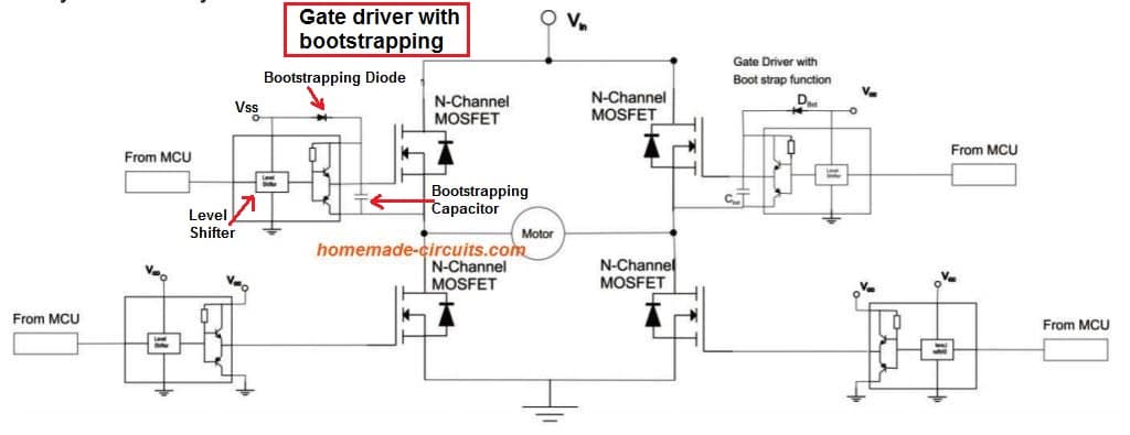
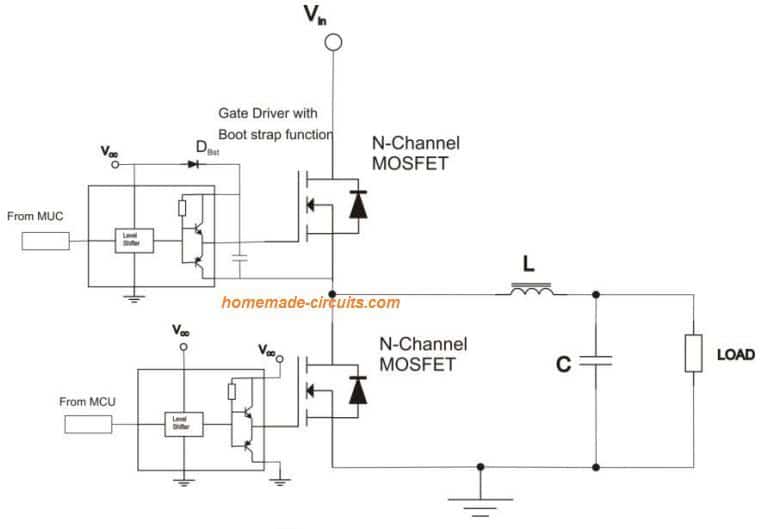
For applying in Low-Voltage Drive networks such as full-bridge or B6-bridge (3-phase bridge) configuration the N-channel MOSFETs are commonly employed with motor (Load) and a DC supply.
The compromising factor for the positive aspects presented by N-channel devices is the higher complexity in the gate driver design.
A gate driver of an N-channel high side switch demands a bootstrap circuit that creates a gate voltage greater than the motor voltage supply rail, or alternately an independent power supply to switch it on. Increased design complexity generally leads to greater design work and higher assembly area.
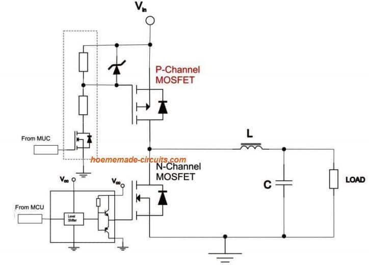
The Figure below demonstrates the difference between the circuit designed using complementary P and N Channel MOSFETs and the circuit with 4 N-channel MOSFETs only.
In this arrangement, if the high side switch is built with a P-channel MOSFET, the driver design simplifies the layout tremendously., as shown below:
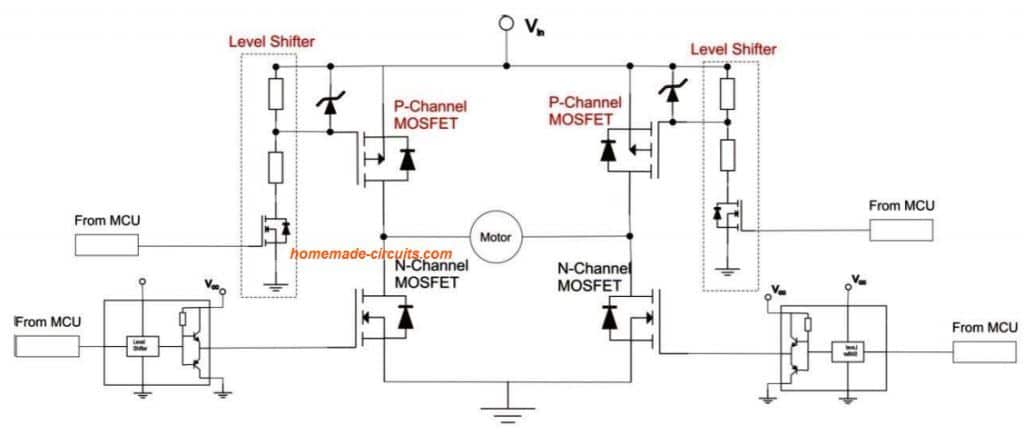
The need for a bootstrapped charge pump is eliminated for switching the high side switch. Here this can simply be driven directly by the input signal and through a level shifter (3V to 5V converter, or 5V to 12V converter stage).
Selecting P-channel MOSFETs for Switching Applications
Typically Low-voltage drive systems work with switching frequencies in the range of 10 to 50kHz.
In these ranges, nearly all of the MOSFET power dissipation occurs by means of conduction losses, because of high current specifications of the motor.
Therefore, in such networks a P-channel MOSFET with appropriate RDS(on) should be chosen to achieve the optimum efficiency.
This could be understood by contemplating an illustration of a 30W Low-Voltage Drive operated with a 12V battery.
For a high side P-channel MOSFET we may have a couple of options in hand - one to have a equivalent RDS(on) comparable with the low side N-channel and the other to have comparable gate charges.
The following table below displays the components applicable for the full bridge Low-Voltage Drive having comparable RDS(on) and with identical gate charges as that of the N-channel MOSFET on the low side.
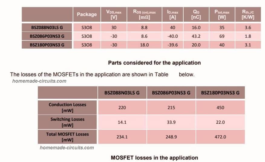
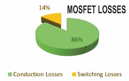
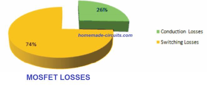
The table above depicting the MOSFET losses within the particular application reveals that the overall power losses are governed by the conduction losses as proven in the following pie chart.
Additionally it looks like if P-channel MOSFET is preferred having comparable gate charges as that of the N-channel, the switching losses will be identical, but the conduction losses may probably be excessively high.
Therefore, for low switching applications with lower frequencies the high side P-channel MOSFET should madatorily have a comparable RDS(on) like that of the low side N-channel.
Non-isolated Point of Loads (POL)
Non-isolated Point of Loads is a converter topology such as in buck converters where the output is not isolated from the input, unlike the flyback designs where the input and outputs stages are completely isolated.
For such Low power non-isolated Point of Loads having output power lower than 10W, presents one of the greatest design difficulties. Sizing has to be bare minimum while preserving a satisfactory degree of efficiency.
One popular way to decrease converter size is to use N-channel mosfet as the high side driver, and increase the operating frequency to substantially higher level. Faster switching allows the use of a much a scaled-down inductor size.
Schottky diodes are often implemented for synchronous rectification in these types of circuits however MOSFETs instead undoubtedly are a better option since the the voltage drop for MOSFETs is usually substantially lower than a diode.
Another space-saving approach would be to substitute the high side N-channel MOSFET with a P-channel.
The P-channel method gets rid of the complex supplemental circuitry to drive the gate, which becomes necessary for an N-channel MOSFET on the high side.
The diagram below demonstrates the fundamental design of a buck converter having a P-channel MOSFET implemented on the high side.
Normally the switching frequencies in non-isolated Point of Load applications will likely be close to 500kHz, or even at times as high as up to 2MHz.
Contradicting the earlier design concepts, the main loss at such frequencies turns out to be the switching losses.
The figure below indicates the loss from a MOSFET in a 3 watt non-isolated Point of Load application running at a switching frequency of 1MHz.
Thus it shows the level of gate charge that must be specified to a P-channel when it is selected for a high side application, with respect to a high side N-channel device.
Conclusion
Applying a P-channel MOSFET no doubt gives you the designers advantages in terms of less complicated, more dependable and an improved configuration.
That said for a given application, the compromise between RDS(on) and QG should be seriously evaluated while selecting a P-channel MOSFET. This is to ensure that the p-channel is able to offer an optimal performance just like its n-channel variant.
Courtesy: Infineon


Need Help? Please Leave a Comment! We value your input—Kindly keep it relevant to the above topic!