The proposed IC 555 based modified square wave inverter circuit generates accurately spaced PWM pulses which imitates a modified sine wave very closely and thus can be considered as good as its sine wave counterpart design.
Here we use two stages for creating the required PWM pulses, the stage comprising the ICs 741 and the other comprising the IC 555. Let’s learn the whole concept in details.
How the Circuit Functions – The PWM Stage
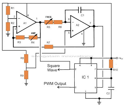
The circuit diagram can be understood with the following points:
The two opamps are basically arranged to generate the required sample source voltages for the IC 555.
The couple of outputs from this stage is responsible for the generation of square waves and triangular waves.
The second stage which is actually the heart of the circuit consists of the IC 555. Here the IC is wired in a monostable mode with the square waves from the opamp stage applied to its trigger pin #2 and the triangular waves applied to its control voltage pin # 5.
The square wave input triggers the monostable to generate a chain of pulses at the output where as the triangular signal modulates the width of this output square wave pulses.
The output from the IC 555 now follows the “instructions” from the opamp stage and optimizes its output in response to the two input signals, producing the sine equivalent PWM pulses.
Now it’s just a matter of appropriately feeding the PWM pulses to the output stages of an inverter consisting of the output devices, the transformer and the battery.
Integrating PWM with the Output Stage
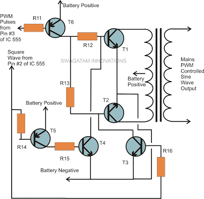
The above PWM output is applied to the output stage as shown in the figure.
Transistors T1 and T2 receive the PWM pulses at their bases and switch the battery voltage into the transformer winding according to the duty cycles of the PWM optimized waveform.
The other two transistors make sure that the conduction of T1 and T2 takes place in tandem, that is alternately so tat the output o from the transformer generates one complete AC cycle with the two halves of the PWM pulses.
Waveform Images:
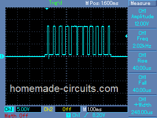
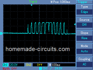
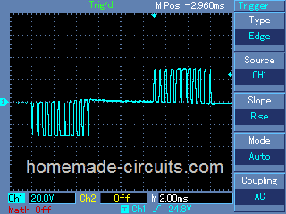
(Courtesy: Mr. Robin Peter)
Please also see this 500 VA modified sine wave design, developed by me.
Parts List for the above IC 555 modified square wave inverter circuit
- R1, R2, R3, R8, R9, R10 = 10K,
- R7 = 8K2,
- R11, R14, R15, R16 = 1K,
- R12, R13 = 33 Ohms 5 Watt,
- R4 = 1M preset,
- R5 = 150 K preset,
- R6 = 1K5
- C1 = 0.1 uF,
- C2 = 100 pF,
- IC1 = TL 072,
- IC2 = 555,
- T1, T2 = BDY29,
- T5, T6 = TIP 127,
- T3, T4 = TIP122
- Transformer = 12 – 0 – 12 V, 200 Watts,
- Battery = 12 volts, 100 AH.
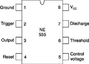
- IC 555 Pinout
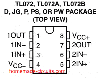
IC TL072 Pinout Details
PWM waveform stands for pulse width modulation waveform and this is applied in the discussed SPWM inverter circuit using a few 555 ICs and a single opamp.



Need Help? Please Leave a Comment! We value your input—Kindly keep it relevant to the above topic!