In this post I have explained how to build a simple yet accurate digital sine wave generator circuit, which is basically an oscillator circuit, enhanced to generate square waves through incrementing steps, which ultimately appears like a stepped sine waveform.
By Ron Mackenzy
The difference between analogue sine wave generator and digital sine wave generator is that, in analogue design mainly op amps are utilized to shape a smooth exponentially increasing pure sine waveform, while in a digital mode, the waveform is also exponentially increasing but it is with a staggered shape, or in a stepped manner.
Advantage
The main advantage of digital sinewave compared to the analogue counterpart is that, analogue sine wave cannot be used to switch MOSFETs or power transistors for a given applications such as sine wave inverters, converters, motor control etc, while digital sine waveform becomes perfectly suitable for such applications, without causing heating up of the devices.
This is because, transistors do not "like" to conduct with analogue signals, or with smoothly rising/falling exponential waveforms, instead the internal characteristics of these devices allow them to be more suitable to logic waveforms, triggered with high and low logic signals.
How the Circuit Works
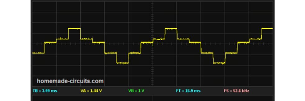
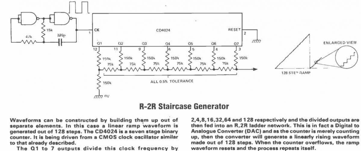
The circuit is made up of a couple of stages, each of which might have several valuable applications by itself: an oscillator built using a set of EX(clusive) OR gates along with a divide-by-three circuit created through a pair of common flipflops.
The basic oscillator consists of a noninverting gate (N1) and an inverting gate (N2). If simply inverting gates was utilized, a minimum of about three might have been required for this oscillator, however, a non-inverting gate could be constructed through a couple of inverting gates hooked up in series.
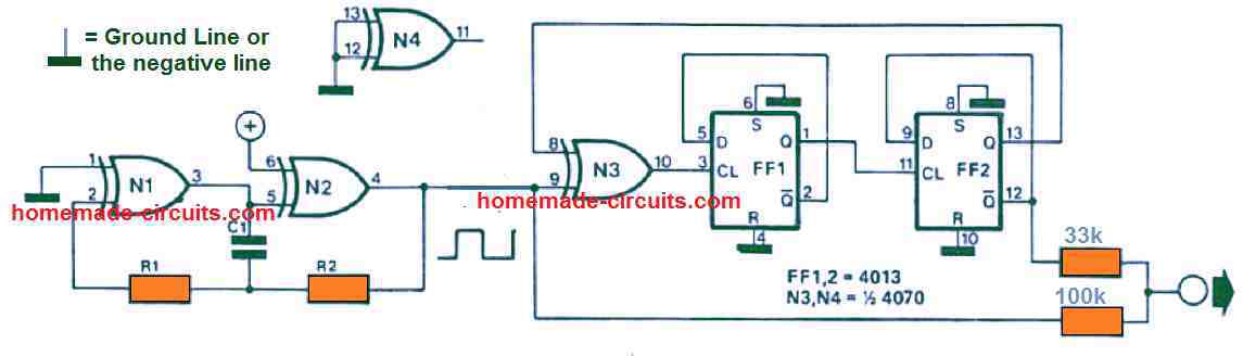
The circuit functions like this: We will suppose that, at the start, the input of N1 (pin 2) is low. Therefore the output of N1 will be also low causing the output of N2 to be high.
Capacitor C1 will subsequently be charged through resistor R2. After a brief moment, the N1 input should go high through R1 and the entire process is going to be reversed. The divide-by-three section includes a couple of flip-flops that each divide by 2. Put simply, it would be anticipated that collectively these might divide by four.
Having said that, an additional EXOR gate (N3) can be seen incorporated between the output of FF2 and the input of FF1. This efficiently inverts the clock input signal whenever the output of FF2 flips its polarity. In case N3 hadn't been used the flipflop's output state wouldn't switch before the ongoing clock interval ended.
With the help of N3, the clock signal gets inverted and its positive-going edge activates the flipflop once every half time period. As a result, the dividing element in the process is three, never four. The sinewave signal is created by using a couple of resistors (R3 and R4).
As soon as the input on the two resistors is low (logic zero) no output voltage will be seen. Once the input to the two resistors becomes high (logic one) the output voltage turns high. If one of the inputs applied to the resistors is low while the other input is high, causes the output voltage to be either 1/4th or 3/4th of the supply (high) level.
Waveform
Surely, the above situation could be confirmed through formulas, but a less complicated technique is to describe this by analyzing just one sinewave interval through a waveform diagram.
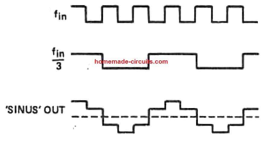
A small rectangle could be used at the center of the sinewave to symbolize a logic 1 level. A pair of additional rectangles of the identical dimension then can be sketched on each side of the first. The region within the sinewave of the final a couple of rectangles is going to be half that of the first. The digital simulation method produces a signal using the exact same regions like the above.
While building this particular digital sine wave generator circuit, it has to be taken into account that CMOS inputs must never be kept 'floating'.
This means that, pins 12 and 13 of the EXOR chip (N4) must be attached to ground (0V).
Stepped Sinewave Voltage Generator Using IC 4046
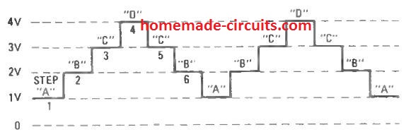
A stepped sinewave voltage generator is an electronic circuit designed to generate a sequentially stepped voltage waveform, which resembles a sinusoidal appearance, but has a stepped voltage pattern ascending sequentially upwards towards the peak and then descending sequentially downward with identical steps towards the 0V line to complete a cycle of the waveform.
How the Circuit Works
The figure below exhibits a useful application of the IC 4066 quad bilateral switch. In this circuit, the 4066 (U1) is configured to carry out sequential switching, in order to generate a uniform stepped waveform; as indicated in the next figure. As demonstrated, the generator's waveform consists of 3-up and 3- down steps through 1V increments.
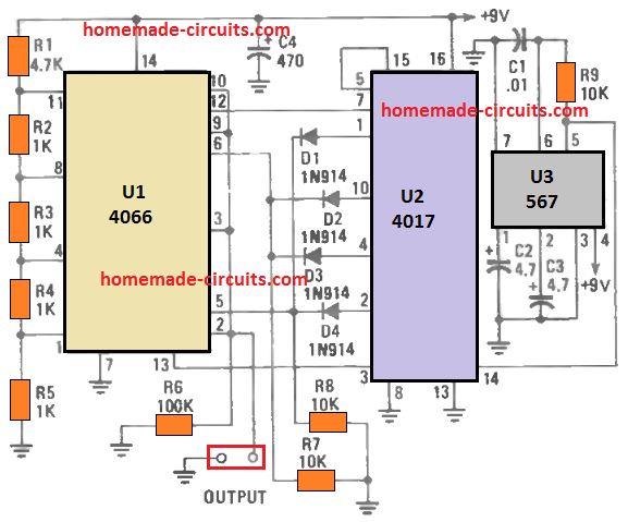
The triggering for the 4066 internal switches is governed by a 4017 decade counter/divider (U2); a 567 tone decoder set up like a squarewave generator provides the required clock pulses for the IC 4017.
The 4017 is rigged to count from 0 to 5 (0-1-2-3-4-5) sequentially and reset on the rising edge of the seventh step by coupling pin 5 (output 6) of U2 to pin 15 (reset).
As soon as output 6 (pin 5 of U2) becomes high, the reset terminal of U2 pushes output 0 (pin 3) to flip from low to high, starting the pattern afresh.
The high pin-3 output (output 0) of U2 is given to the control pin of the 1st U1 switch, switching it on and consequently connecting the intersection of R4 and R5 with the output bus.
This sets up step one with a one-volt level. With the following clock pulse from the 567, the 4017 generates a high output at pin 2, which is applied via D4 to another switch control at pin 5, switching it on.
This links the R3, R4 with the output bus. The 2nd step constitutes a 2-volt output. For the subsequent pulse obtained via U3, pin 4 of U2 turns high, evoking the 3rd switch (in U1) to activate, which respond to generate a 3- volt output intended for step 3.
The 4th pulse coming from U3 results in pin 7 to become high, switching on the very last switch, and thus creating a 4-volt output for step 4.
The fifth pulse feeds a high to pin 10 of U2, which moves by means of D4 to the control input of the 3rd switch, switching it on (for a second occasion) and providing a 3-volt output to the 5th step.
For the subsequent clock pulses, the switch attached to pin 6 of U1 is yet again activated, generating a 2-volt output for step 6. Soon after step six is accomplished, the counter resets and commences back from the start by switching on the 1st switch for step 1.
Each waveform step can be arranged for any voltage right from zero to 100 % supply voltage through the use of specific voltage dividers for each step. Additionally, the generator's output could be buffered to deliver adequate voltage and current outputs to provide rising voltage or current supply for a semiconductor curve tracer.
Another Simple Stepped sine wave Voltage Generator using IC 4017
The next design below is even simpler to build as it employs just a couple ICs for the required stepped waveform creation.
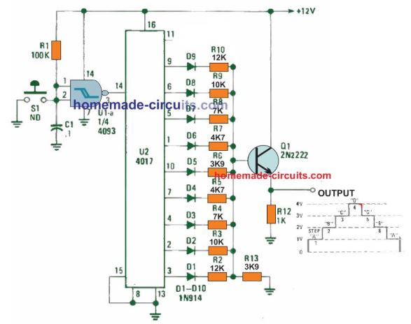
However, the stepped sine wave generator design is implemented in a manual mode, wherein the sequential steps of the waveform are developed by tapping the push button S1 at a specific timed rate. Each pressing causes the output of the IC 4017 to shift from pin3 upwards, towards pin11.
In the process, the common ends of the resistors happen to develop a sequentially ascending and descending stepped voltage due to the effect of the varying potential divider formed by the interaction of the shifting IC 4017 logics across the resistors R2---R10 and the ground resistor R13.
Since the common joined ends of the resistors are together fed to the base of a common-emitter BJT stage, the stepped voltage is replicated at the emitter of the 2N2222 transistor with a higher current level, which can be integrated with any suitable external circuit stage for a desired execution.
The manually controlled switch can be replaced with an automatic oscillator stage as indicated in the following example, which shows the implementation of the above stepped voltage generator in a police lamp effect simulator circuit.
Applications
You will find a variety of applications for this circuit. The stepping sine waveform generator could be implemented to produce numerous progressive voltages for examining the on/off switching point of many CMOS units. It can be effectively used for making efficient sine wave inverters and converters.
Application Circuit
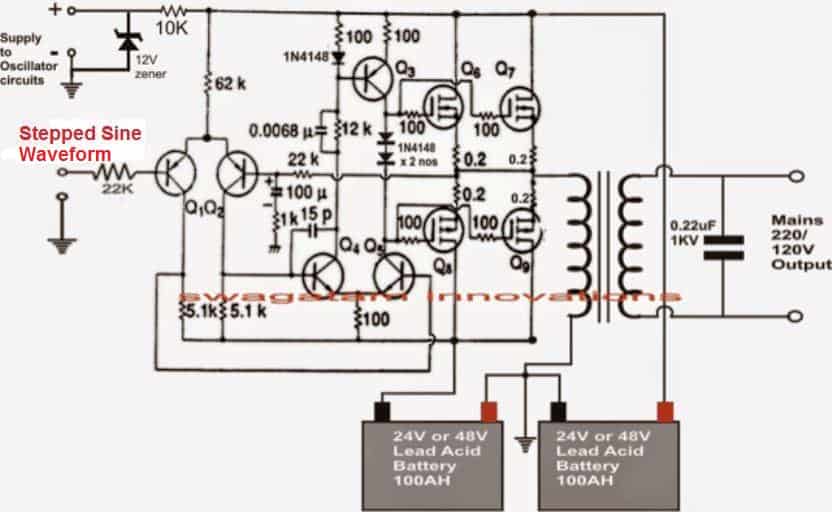
A stepped waveform can be very effectively used for making a sine wave inverter as shown in the following example:
Comments
Thank you so much Mr Swagatam, you really are my mentor!. I have built a lot of inverters under your guidance, however I’ve not been able to produce a single pure sine wave inverter due to the complex nature. Can you help me with a logic ic based sine wave generator circuit, such that when I implant it in my inverter circuits, I’ll get a pure sine inverter?. I’ll appreciate if you’ll do me this favour. Thanks
Thank you Chinomso,
Actually it is not possible to feed a pure sine wave to create a sine wave inverter.
Instead you will need an SPWM or sine PWM waveform to convert it into a sine wave inverter.
If you want to integrate a sine wave system to an existing inverter, the best way is to integrate a SPWM chopping with the MOSFETs