In this post I have explained how to build 6 useful voltage controlled oscillator circuits, using various op amps and integrated circuits.
As the name suggests, a voltage controlled oscillator or a VCO circuit is an oscillator circuit whose output frequency can be controlled or varied through an adjustable control voltage input. This means, if the input control voltage is increased, the output frequency will increase proportionately, and vice versa.
If the control voltage varies continuously up and down, then the output frequency will also correspondingly increase and decrease, in response to the varying amplitude of the control voltage levels.
Just like any other VCO circuit, in the discussed circuit below, the output frequency is determined by the level of the control voltage applied.
1) Main Features (Using IC LM558)
- The main advantage of this VCO design is that it comes with a wide control voltage range, which extends right from 0 V up to the maximum positive supply voltage limit. The power supply level could be anything from +3V to +25 V.
- Additionally this voltage controlled oscillator (VCO) is designed to generate both triangular as well as a square wave output signals.
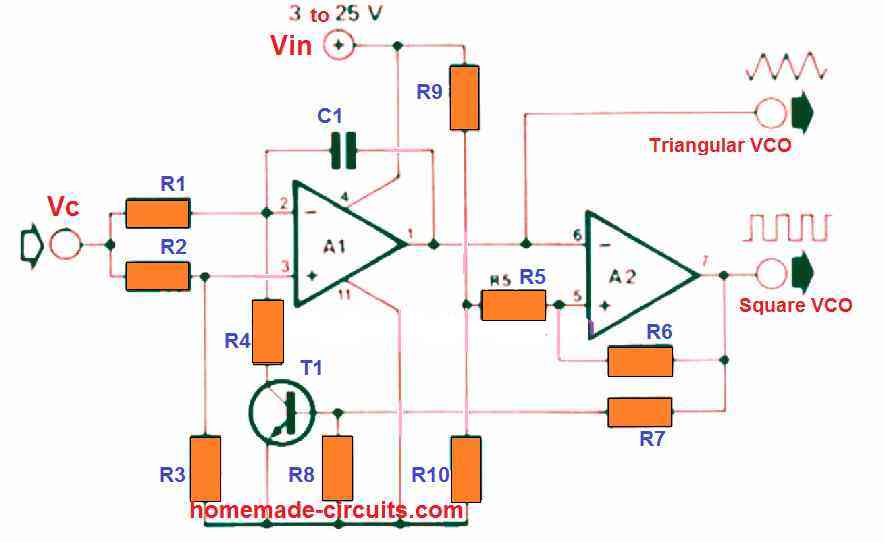
Parts List
- R1, R5, R6 = 100K
- R2, R3, R4 = 47K
- R7, R8, R9, R10 = 10K
- C1 = 47 nF
- T1 = BC547
- A1, A2 = LM358
Having said that, the user has to be careful while working with low voltage inputs, and ensure that the highest input voltage level is at least 1.5 V lower than the supply voltage.
How the Circuit Works
The circuit functions by using the 'integrator/comparator' theory. Capacitor C1 forms the part of the integrator (designed around opamp A1), and it is charged using a constant current source as determined by the instantaneous level of the applied control voltage.
As a result, the A1 output voltage falls linearly. The comparator output (built using A2) changes state and transistor T1 begins conducting as soon as the comparator's bottom switching threshold is attained.
Capacitor C1 at this point is discharged, triggering the A1 output to increase (again, this rising voltage is linear in nature). The action repeats, and the moment the A1 output extends to the comparator's upper switching limit, it switches OFF T1.
The duty cycle of the output voltage controlled frequency is going to be FIFTY PERCENT if the R2 and R3 values are identical (R2 = R3), and when the value of R1 is two times than that of R4 (R1 = 2 x R4).
The relationship between the R9 and R10 values becomes responsible for the level of the triangular DC output voltage.
With respect to the R9/R10 values shown in the schematic, the triangular DC level will likely be 1 / 2 the supply voltage. The peak-to-peak output level, can be determined by solving the following equation:
(Vpp) = R5 / (R5 + R6) x Vin
Control Voltage, Supply Voltage Relationship
The characteristics of the proposed voltage controlled oscillator or the VCO using a pair of (common) supply voltages can be witnessed in the following graph.
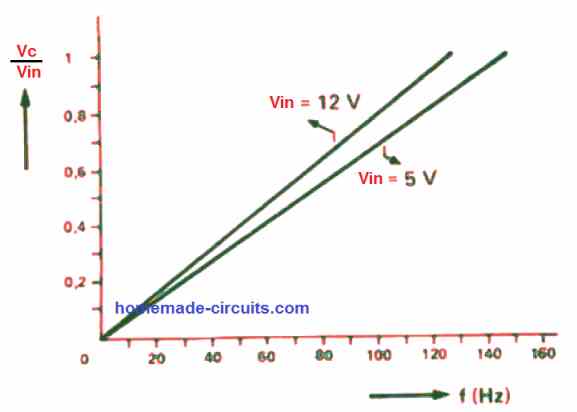
When both the supply inputs are equal (Vin = Vc) in magnitude the maximum frequency that can be achieved from the circuit could be increased or decreased by correspondingly selecting the C1 value lower or higher. With regards to the opamp's slew rate, the vertical angle of the squarewave signal may decline for the higher frequencies.
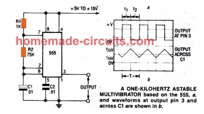
2) VCO using IC 7555
A neat little voltage controlled oscillator can also be built using the resolute IC 555 and a few other assisting components, as shown below:
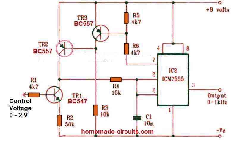
The discharge process of capacitor C1 is voltage controlled. This is implemented by the quick charging pulses controlled by the internal discharge transistor of IC2.
To understand the working, imagine the pin3 output of timer IC2 is initially low and the discharge transistor pin 7 is switch ON, pulling current through R6 to activate transistor TR3. This particular transistor maintains the transistor TR2 base at the positive supply voltage. This guarantees that it is switched off.
The capacitor C1 may consequently start discharging via R4 with a rate as decided by the TR1 collector current. As the voltage across C1 drops to around 1/3rd supply voltage level, the IC555 output turns high. Simultaneously the discharge transistor along with TR3 also switch OFF, which means that current through R3 now activates TR2, which begins charging C1 via R4.
As soon as the voltage across C1 gets to 2/3rd of the supply voltage, IC2 yet again changes state and the cycle keeps repeating. A functioning property of transistors is such that practically all the current going to the emitter side, runs out back from the collector. A tiny amount of current passes out from the base, however normally, this is very small to be considered.
Due to the fact that the emitter voltage follows the applied base voltage, deducting the base/emitter forward drop of around 0.6 volts, this voltage output enables you to control the voltage over the emitter resistor R2 with this circuit. The transistor base voltage as a result controls the collector current, giving rise to a voltage controlled current source.
The control voltage could be applied directly on the transistor TR1 base in order to control the frequency output in this circuit.
3) Using Op amp with IC 555
In another situation, if an op-amp is employed with the transistor as displayed in the next diagram below, then the voltage across R2 may follow accurately the input voltage, and the the op-amp would automatically begin compensating for the emitter-base voltage drop as well as disparities due to temperature changes. The resulting output frequency control range can then begin from zero rather than 0.6 volts.
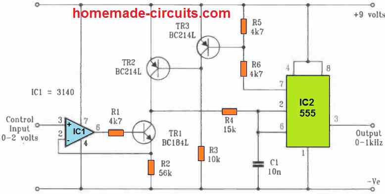
Calculations required for designing this IC555 based VCO circuit can be as easy as for the simple fixed-frequency circuits, which means just a couple of rules must be followed. Resistor R4 has to be relatively low in values compared to the value of R2.
There should always be sufficient voltage across TR 1 for it to work, therefore the input must in no way cross 1 V value below 1/3rd supply voltage. This particular voltage controlled oscillator circuit is vulnerable to variations in the supply voltage, therefore the supply should be strictly regulated.
Once the maximum control voltage range is fixed, the period for the discharge element of every single cycle could be worked out using the formula:
t = (C x R x E) / V
Here C represents the timing capacitor C1, R stands for the emitter resistor R2, E indicates 1/3rd of the supply level and V represents the voltage across R2.
To th result from the above expression, we have to add the time taken for the charging portion of the cycle:
t = 0.7 x C1 x R4
The two elements collectively provide the full period for each cycle hence, as a common practice, their inverse provides the equivalent frequency. With the part values indicated with a 9 V supply input, the circuit produces a frequency response from 0 Hz to approximately 1 kHz in response to an input control voltage between 0 to 2 volts.
The output frequency is composed of positive pulses of 100 us width, excellent for generating a wide range of noise over a small loudspeaker using the most basic of output buffer stages, maybe just one BJT stage. Using C1 as a 1 nF capacitor it delivers approximately 9 kHz for exactly the same input voltage range, using proportionately shorter output pulses.
Which Opamps are Suitable
Remember that in case an op-amp is employed as indicated in the above VCO circuit diagram, it has to be of a kind having input and output rated to work right down to the negative supply voltage. The IC CA3140 as indicated is acceptable, some other possible variants could be the CA3130, or one of the op amps from the IC CA3240, LM358 or LM324.
Various other transistors may also work very well instead of the one shown in the diagram, as long as these are assembled with the proper polarity.
The practical use of this IC 555 voltage controlled oscillator circuit may not be extensive, and may be restricted to generally with audio related work, but the design is very cheap, straightforward and pretty stable with its specifications.
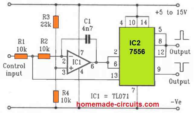
4) Using IC 7556
In the previous voltage controlled oscillator circuit, transistors were employed to provide a steady current and to reverse the discharge signal from a timer IC. To show what's possible, here's a VCO design that uses an op-amp integrator instead of a timing capacitor and current source, plus an IC7556 dual timer for inversion. An op-amp integrator includes a couple of inputs: one that is non-inverting and generally linked to a reference voltage, and the other that is inverting and coupled to an input voltage via a resistor, with a negative feedback from the output, provided by a capacitor.
The op-amp utilizes feedback to maintain the voltage at the inverting input same as the voltage at the non-inverting input, within the limits of the supply voltage.
If a constant voltage is given to the input resistor, the voltage across it will equal the difference between this and the reference voltage, resulting in a constant current flowing into the input. This current charges the feedback capacitor. As a result, the op amp output voltage varies at a stable rate to maintain the inverting input voltage constant.
This may be implemented to make an oscillator by changing the input voltage polarity when the output goes over the timer IC's input limits. One small snag is that the integrator output is reversed, with positive inputs dropping and negative inputs rising.
There has to be a polarity inversion at a certain point in order to build a working oscillator with the inverting IC7556. A dual op-amp, with the latter inverting the output of the first, is one way of achieving this. Nevertheless, this necessitates the addition of a minimum of two extra resistors, which can compromise the circuit's frequency.
A better solution is to utilize two timers, with the second one serving as an inverter for the first's output. Figure 1.5 depicts a circuit that works in this manner. IC1 is the integrator, having resistors R3 and R4 providing a reference voltage of roughly 1/3 of the supply voltage to its non-inverting input pin3.
A voltage larger than the reference supplied to resistor R1 while the discharge transistor of the second timer, pin 13, is switched off would make the output of IC1 to drop at a rate specified by the input voltage and the values of Rt, R2, and capacitor C1. The first timer switches state as soon as it approaches 1/3 of the supply voltage, with output pin 5 becoming high.
Because this is linked to the second timer's inputs, pins 8 and 12, the output of this is now becomes low, and the discharge transistor, pin 13, is turned on. The integrator's output begins increasing, since it has an apparent negative input of roughly a 1/3 of the supply linked to R2. The two timers swap states again the moment it reaches 2/3 of the supply voltage, and the process continues. The time for the first part of the cycle is calculated as follows:
t = C x R x V / E
Where C represents C1, R1 represents R1+ R2, V represents 1/3 of the voltage supply, and E represents the supplied input voltage.
A similar equation may be used to compute the time for the second portion of the cycle in this situation. Because R is R2 by itself and V and E are almost identical in value, the time may be calculated as follows:
t = C1 x R2
5) VCO using IC CA3130
Even though this Voltage Controlled Oscillator works by using just a couple of CA3130 op amps, it is still able to exhibit a voltage/frequency linearity transfer characteristic far better than 0.5%, while its temperature coefficient remains lower than 0.01%/°C.
The working of the circuit can be understood wit the following points: IC1 operates like a voltage controlled multivibrator. Supposing that the IC1 output voltage is +15 V at the start, C1 begins charging through D3, R4 and P1 by means of a time constant components (R4 + P1) C1.
C1 keeps charging until the potential across the IC1 inverting input surpasses the potential on the non-inverting input. Ignoring the diodes D1 and D2 momentarily, we get around 10 V, fixed by the resistive divider network R1, R3 and R2.
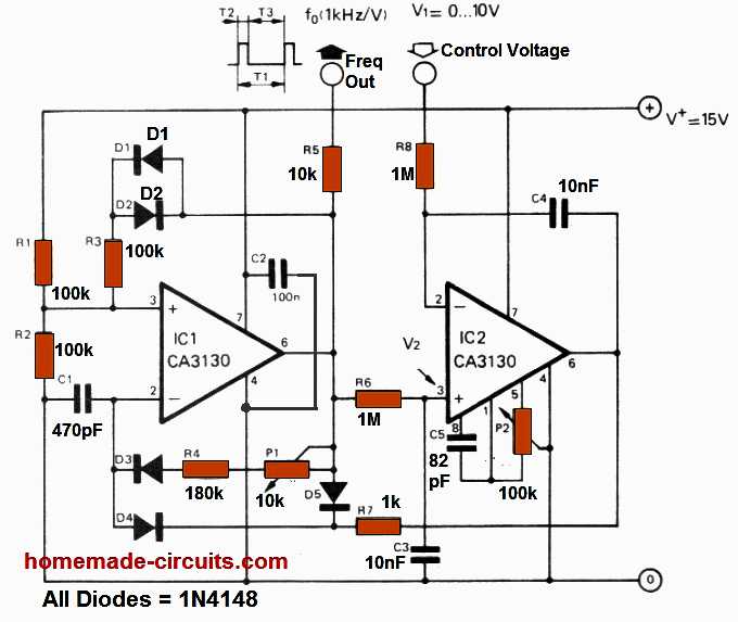
The IC1 output now instantly switches down to 0 V, and the potential at the non-inverting input of the IC drops to approximately 5 V as a result of the hysteresis presented by R3.
Next, capacitor C1 begins discharging through IC2 output at a rate depending on the value of the resistor R7 and via the output voltage of IC2. This continues until the potential at the IC1 inverting input drops under 5 V. As soon as this happens, the IC1 output instantly turns up to +15 V once again and this cycle goes on repeating.
The waveform generated at the output of IC1 therefore exhibits a train of positive pulses with a time interval (T2) which is constant and whose pulse width (T1) determined by the IC2 output voltage.
The resistor R6 and capacitor become responsible for filtering the the IC1 output voltage providing a DC voltage (V2) that's equivalent to the average value of the IC1 waveform, which can be expressed by the formula:
V2 = 15 x T2/T1
Given that T2 is constant, V2 will be proportional to 1/T1, meaning this will be proportional to the output frequency generated from IC1. The control voltage V1 is fed on the inverting input of IC2, which is wired like an integrating comparator.
While V1 is lower than V2, causes the IC2 output to generate a positive ramp. This in turn causes C1 to discharge with a sluggish rate, resulting in the T1 time interval to be longer, and V2 to decrease.
When V1 goes higher than V2 causes the IC2 output to generate a negative ramp (i.e. in direction of zero) forcing C1 to discharge faster and a decrease in T1.
If V1 and V2 are identical, the voltage from IC2 stays constant. The VCO circuit thus always tends to acquire an equilibrium whenever V1 = V2.
That said, considering that V2 and the output frequency of IC1 are proportional, that means the IC1 output frequency will also be proportional to the input voltage V1, given that V1 and V2 are identical. Some minor improvements are included to enhance the temperature stability of the voltage controlled oscillator.
The temperature coefficients of D3 and D4 might possibly cause glitches by altering the charge and discharge periods of C1, therefore their effects are adjusted by incorporating diodes with similar characteristics in series with the resistor R3 to enable an equivalent counter deviation in the reference voltage at the non-inverting input of IC1.
Preset P2 can be used to adjust the offset voltage of IC2 to zero. The preset P1 allows minute adjustment of the conversion ratio, which through the indicated values can be approximately 1 kHz/volt
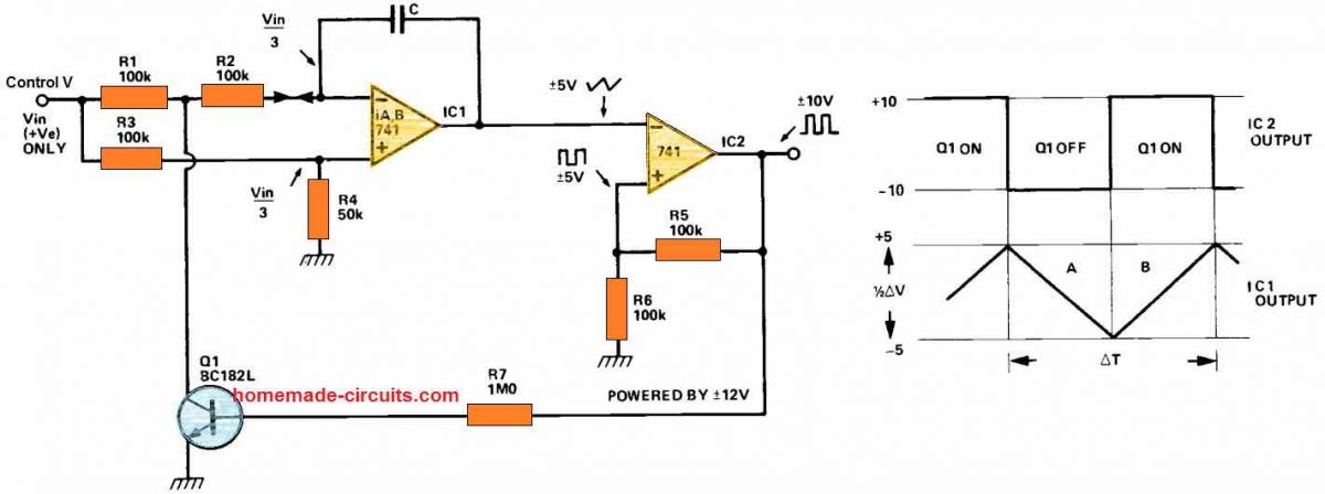
6) Simple Linear VCO Circuit
The next figure depicts yet another simple linear VCO. A couple of buffered outputs, a triangle and a square wave, can be seen in the design. Likewise, the oscillation frequency is determined by the Schmitt trigger's output voltage variation, IC2. When a stabilized power source is provided, then, this circuit performs admirably.
Q1 can be replaced with a switching FET for improved working performance. The degradation triggered by saturation voltage and storage time are consequently eliminated. High-frequency performance can be also benefited from high speed FET op amps.
7) VCO Application: Audio Tone based Voltmeter
The following concepts explains how a VCO can be used for making an audio tone based voltmeter circuit.
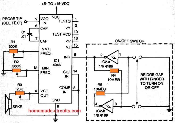
The tone voltmeter circuit is depicted schematically in the picture below. The circuit is constructed around a CD4046B phase-locked loop (PLL) integrated circuit with a built-in voltage-controlled oscillator (VCO).
The voltage level at pin 9, value of capacitor C1 between pins 6 and 7, potentiometer R1 setting at pin 11, and potentiometer R2 at pin 12 control the frequency of the VCO.
The VCO output (pin 4) is usually routed back into the comparator input (pin 3). In this circuit, although, the VCO output powers a loudspeaker directly. Once the inhibit line (INH) at pin 5 is logic low, the VCO activates, and it switches off when INH is logic high.
When the tone voltmeter is not being used, a touch switch made up of two Schmitt-trigger inverters (IC2 -a and -b) switches the circuit on and off to save power. If necessary, the touch switch could be substituted with a conventional SPST switch. Assuming you don't have a Schmitt-trigger inverter and don't want to buy one, this is indeed a good option.
If a logic low is appears at pin9, the circuit generates a low frequency tone. As the voltage input at pin9 grows, so does the pitch of the tone, until the input voltage hits a logic high. Conversely, the tone pitch lowers as the voltage input at pin9 decreases.


Comments (9)
Hi, I built the 3 transistor vco with 7555, i built a few but the output never goes to zero, always 1 hz output, i suspect transistor leakage current is the cause, i can stop this by connecting 1.5 M ohm between 5 and 6 but the linearity is very bad, did you find this when you built the circuit? I built both the opamp input voltage one and the transistor input one, I even shorting out TR1 the oscillator is still running at a low pulse rate.
It could be happening due to the following reasons:
The control voltage which goes from 0 to 2 volts, might not be fully turning off the transistor TR1 (BC547). This transistor is in charge of how the capacitor C1 charges and discharges. Because of this there could be a minimum frequency limit that the circuit cant go below.
The resistors R3, R4, and R6 are important for deciding how capacitor C1 charges and discharges. These resistors might be stopping the capacitor from completely stopping its charging and discharging especially at very low frequencies.
The IC7555 chip has some limits when it comes to making very low frequencies. These limits depend on the specific capacitance and resistance values chosen for the circuit.
You can probably solve it with the following methods:
Try increasing the values of resistors R4 and/or R3. This change will make the time constant of the circuit longer allowing it to produce lower frequency outputs.
Choose a bigger capacitor like one that is 100 nF or more to help create longer charging and discharging cycles.
Make sure that the control voltage can fully turn off TR1. If it can’t then you might need to change the values of resistors R1 and R2 to adjust the base drive signal to TR1.
If the circuit can’t reach a frequency of zero try adding a diode in series with the control voltage input. This could improve the control range and make the circuit work better.
Hello
Can you share the resources of these circuits please? Because I need to know the theoretical expression of the frequency f in terms of the Voltage Vin and the other components like R and C.
Thank you
Sorry, I do not remember it now. The article was actually contributed by another author.
Hi, you seem to have a contradiction when describing the first circuit: you say it features a rail to rail input range, then say that a caveat is that the cv upper limit is Vcc – 1.5 volts.
Wells
The statement refers to the input signal voltage at R1/R2 junction, which is supposed to be lower than the supply voltage by 1.5 V
I have a question about the first circuit (with LM358)!
There is in the circuit diagram Pin11 to ground and Pin 4 to plus.
The LM358 only has 8 connections (DIP8) and 4 should actually be Ground (GND).
What’s wrong here?
Ich habe da mal eine Frage zur ersten Schaltung (mit LM358)!
Da steht im Schaltplan Pin11 auf Masse und Pin 4 an Plus.
Der LM358 hat nur 8 Anschlüsse (DIP8) und 4 sollte eigentlich Ground (GND) sein.
Was stimmt hier nicht?
The shown opamps are actually from IC LM324, but you can use LM358 also, just modify the supply pins accordingly.
Trying to design a 5v feed stepped up to 5kv plus & 5kv minus AC @ 28khz frequency both sine waves are 180 degrees apart output very low amps 2-3 mili amps. Do you have better suggestion how I can make this work safely?