In this post I will comprehensively discuss a 3 basic proximity sensor circuits with many application circuits and detailed features of the circuit.
The first two capacitive proximity sensor circuits uses a simple IC 741 and IC 555 based concepts, while the last one is a bit more accurate and incorporates a precision IC PCF8883 based design.
Working Principle
The following capacitive proximity sensor circuits respond to a human hand by recognizing variations in capacitance when a hand gets closer.
Based on these adjustments, it produces an electrical signal showing the existence and closeness of the hand. Touchscreens and buttons that respond to touch frequently employ this kind of sensor.
Due to the hand's dielectric characteristics (ability to retain electrical charge), when a human hand comes close to the sensor, it changes the capacitance between the sensing electrode and the hand.
The capacitance of the sensor is altered by the human body's conductivity.
The sensor circuit tracks the capacitance in real-time. The capacitance varies depending on how close or far the hand is to the sensor.
The sensor circuit recognizes and switches ON a relay in response to these variations in hand capacitance.
1) Capacitive Touch Sensor Using IC 741
The circuit I have explained below could be configured to activate a relay or any suitable load such as a water tap, as soon as human body or hand comes near the capacitive sensor plate.
With specific conditions the hand proximity is only enough to trigger the circuit output.
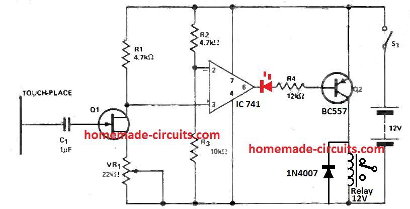
A high impedance input is given by Q1, which is an regular field effect transistor like 2N3819.
A standard 741 op amp is employed in the form of a sensitive voltage level switch which subsequently drives the current buffer Q2, a medium current pnp bipolar transistor, thus activating the relay that may be accustomed to switch a device, such as alarms, faucet etc.
While the circuit is in the idle standby condition, the voltage at pin 3 of the op amp is fixed at greater than the pin 2 voltage level by appropriately adjusting preset VR1.
This makes sure that the voltage at the output pin 6 will be high causing transistor Q2 and the relay to remain switched off.
When the finger is brought in close proximity to the sensor plate or lightly touching, a lowering opposite bias VGS will increase the drain current of the FET Q1 and the resulting drop across R1 voltage will reduce the op amp pin 3 voltage below the voltage existing at pin 2.
This will result in the pin 6 voltage to fall and consequently switch on the relay by means of Q2.
Resistor R4 might be determined in order that the relay is kept turned OFF under normal conditions, considering that a tiny positive off set voltage might develop at the op amp pin 6 output even if the pin 3 voltage happens to be lower than pin 2 voltage in the quiescent (idle) state.
This problem could be remedied simply by adding an LED in series with the Q2 base.
2) Capacitive Touch Sensor Using IC 555
The post explains an effective IC 555 based capacitive proximity sensor circuit which may be used for detecting intruders near a priced object such as your vehicle. The idea was requested by Mr. Max Payne.
The Circuit Request
Hello Swagatam,
Please Post a Capacitive/Body/ Sensitive Circuit can be applied on bicycle. Such device seen on car security system, When somebody come closer to car or a simple 1 in ch proximity would trigger the alarm for 5 seconds.
How this type of alarm works, the alarm only trigger when somebody come closer (say 30cm) what type of sensor they use?
Circuit Diagram
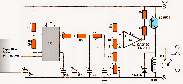
Circuit Image Courtesy: Elektor Electronics
The Design
The capacitive sensor circuit may be understood with the help of the following description:
IC1 is basically wired as an astable, but without incorporating a real capacitor. Here a capacitive plate is introduced and takes the position of the capacitor required for the astable operation.
It must be noted that larger capacitive plate will produce better and much reliable response from the circuit.
Since the circuit is intended to work as a vehicle body proximity alert security system, the body itself could be used as the capacitive plate, and it being huge by volume would suit the application quite well.
Once the capacitive proximity sensor plate is integrated, the IC555 comes into a standby position for the astable actions.
On detecting a "ground" element at a close proximity, which could be the hand of a human, the required capacitance is developed across pin2/6 and ground of the IC.
The above results in an instantaneous development of frequency as the IC starts oscillating in its astable mode.
The astable signal is acquired at pin3 of the IC which is appropriately "integrated" with the help of R3, R4, R5 along with C3----C5.
The "integrated" result is fed to an opamp stage rigged as a comparator.
The comparator formed around IC2 responds to this change from IC1 and translates it into a triggering voltage, operating T1 and the corresponding relay.
The relay may be wired with a siren or a horn for the required alarming.
However it's seen practically that IC1 produces a peak positive to negative voltage pulse at the instant when a caapcitive ground is detected near the plate.
IC2 solely responds to this sudden rise in the peak voltage for the required triggering.
If the capacitive body continues to be at the close proximity of the plate, the peak frequency voltage at pin3 vanishes to a a level which may be undetectable by IC2, rendering it inactive, meaning the relay stays active only at the instant the capacitive element is brought or removed near the plate surface.
P1,P2 may be adjusted for acquiring maximum sensitivity from the capacitive plate
For obtaining a latching action, the output of IC2 may be further integrated to a flip flop circuit, making the capacitive proximity sensor circuit extremely accurate and responsive
3) MOSFET Capacitive Proximity Sensor with Alarm
The next proximity detector circuit exploits the extremely high input impedance and high power features of the FET to create an easy, yet very sensitive, proximity sensor and alarm driver circuit.
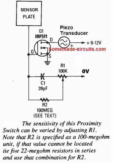
The sensor is formed by a 3x3 inch metal object which is hooked up with the Q1 gate.
The resistor R2 which is a 100 M resistor, separates the Q1's gate from R1, permitting its input impedance to stay extremely high.
If you are unable to find a 100 M resistor, you may simply connect five 22 M resistors in series and work with this resistor string instead of R2.
Precisely speaking , R2 value could be created even higher than this for enhancing the proximity detection sensitivity.
Potentiometer R1 is adjusted to a point where the piezo buzzer just starts buzzing ON and then R1 could be meticulously adjusted back to the point where the buzzer just stops sounding anymore.
Testing with the R1 adjustment can be useful in having the greatest sensitivity setting for this capacitive proximity circuit.
4) Using a Single FET
The next circuit depicts a load-sensitive capacitive proximity sensor circuit, which employs a BC170 N-type FET as the active device.
This is an extremely robust and sensitive proximity-sensor circuit that may be used in security devices and industrial applications.
A Hartley oscillator having adjustable feedback gain control is used in this design.
A hand-wound inductor replaces the RC frequency-determining components utilized in our prior device.
The frequency of the oscillator is governed by L1's inductance, internal capacitance, and the sensor plate's load capacitance.
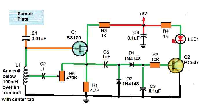
R5 controls the feedback gain required to achieve and maintain oscillation.
C5 couples the oscillator's output signal to a rectifier circuit, which provides a positive bias to toggle Q2 on and illuminate the LED.
Gently adjust the potentiometer until the LED slightly begins to light, with R5 adjusted to its greatest resistance value.
The sensor's highest sensitivity is at this point.
In the circuit, any center-tapped inductor with an inductance value between 0.1 and 100 mH should suffice.
Our circuit's coil was made up of 120 turns of 28-gauge enamel coated copper wire "jumble coiled" on a 1-inch pipe.
Take a tap at the 60th turn and keep winding for yet another 60 turns.
Because the actual inductance value isn't important, any pipe bobbin of comparable size would suffice for the shape; the thickness of the wire used can also vary.
5) Capacitive Motor Controller Circuit
This circuit represents a capacitive touch switch designed for the purpose of controlling 12 Vdc motors.
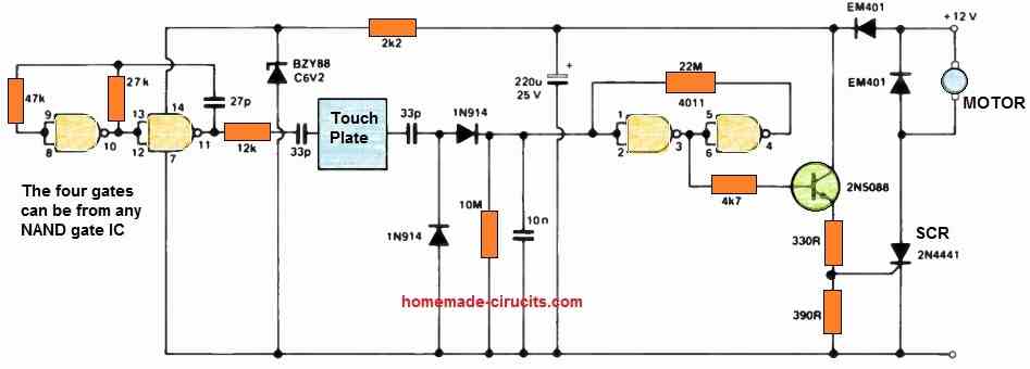
An ideal application for this switch is to install it on a storefront window, enabling the manipulation of a display using a car electric fan motor.
The operation of this circuit involves an oscillator that drives a touch plate securely adhered to the inner surface of a glass window.
The entire circuit is capacitive in design, making it well-suited for controlling 12 Vdc motors.
This configuration lends itself to versatile applications, particularly when interfacing with small dc motors requiring 400 mA at six volts, such as those commonly found in Fisher Technic devices.
The output functionality of this circuit relies on logic signals applied to inputs A and B, as detailed in the accompanying reference table.
The construction of this circuit is straightforward, and it necessitates minimal or no heat dissipation measures due to the transistors' ability to operate either in a fully saturated state or turned off.
Input involves grounding a 50 mm diameter touch plate, causing the Schmitt trigger to activate the SCR (Silicon Controlled Rectifier).
To ensure extended operation even after releasing the touch plate, a 10nF capacitor is integrated into the design.
It's important to note that since the SCR latches on with a dc supply, it is recommended to use an unregulated and unfiltered power supply for this application.
For situations requiring intermittent operation, there is no need for additional heatsinking, resulting in a compact circuit design that is smaller in size than the touch plate itself.
The compact dimensions allow for the entire switch to be enclosed in a sealed plastic casing, offering protection against environmental humidity.
6) Wide Voltage range Capacitive Switch Sensor
Most capacitive touch switch circuits typically employ a comparator, necessitating constant adjustments to the reference input, especially when the supply voltage changes.
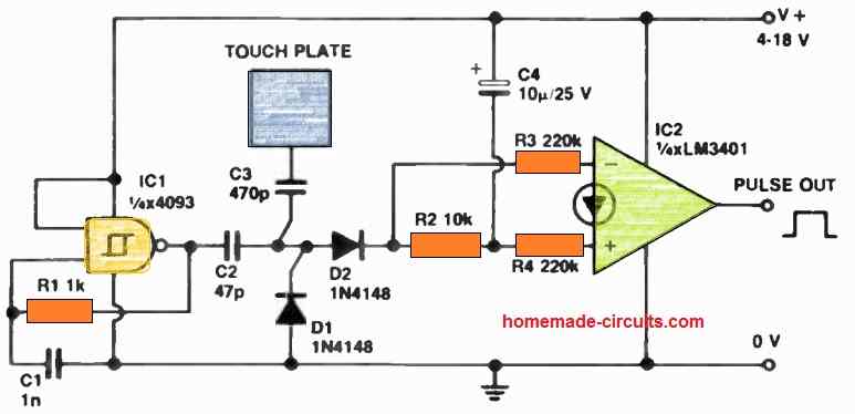
My aim was to circumvent this requirement, making these switches suitable for logic design applications with variable power supplies across the CMOS range.
The resulting circuit eliminates the need for ongoing adjustments and functions seamlessly within a voltage range of 4-18 V, spanning from the lower limit of the op-amp to the upper limit of the Schmitt trigger.
Here's how it works:
The output from the Schmitt trigger astable circuit, including components IC1, R1, and C1, feeds into the capacitive divider composed of C2 and C3.
After rectification, the signal is directed to both inputs of the Norton op-amp comparator.
While the capacitive divider principle is a well-established concept, the specific manner in which it's applied in this circuit is an original idea.
R2 serves to bias the non-inverting input slightly below the inverting input, resulting in a normally low output.
When the capacitive plate is touched, causing a voltage drop, this change in voltage is sent to both inputs.
However, there's a delay introduced by R2 and C4 in the non-inverting input, causing the inverting input to momentarily dip below the non-inverting input.
This triggers the op-amp for that brief duration, generating a short positive pulse at the output.
The op-amp operates effectively across nearly the entire supply range, yielding a relatively clean pulse with minimal switch bounce.
This pulse can serve various purposes, such as triggering a monostable circuit, being squared up by a Schmitt trigger, or utilized in an op-amp or JK flip-flop toggling circuit, among other control functions.
It's worth noting that an LM3900 can be used as a substitute for the LM3401.
Since both the op-amp and Schmitt trigger are available in quad packages, this circuit design is particularly well-suited for applications involving sets of four switches.
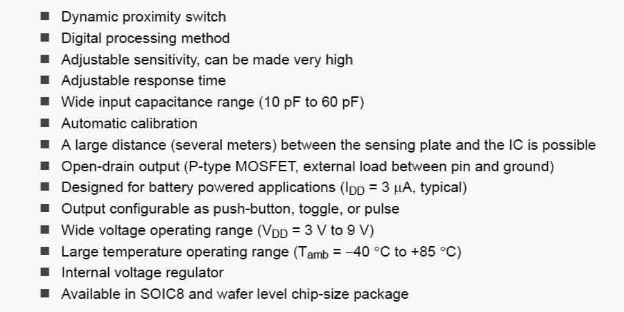
7) Using IC PCF8883
The IC PCF8883 is designed to work like a precision capacitive proximity sensor switch through a unique (EDISEN patented) digital technology for sensing the minutest difference in the capacitance around its specified sensing plate.
Main Features
The main features of this specialized capacitive proximity sensor can be studies as given below:
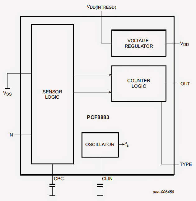
The following image shows the internal configuration of the IC PCF8883
The IC doesn't rely on the traditional dynamic capacitance mode of sensing rather detects the variation in the static capacitance by employing automatic correction through continuous auto-calibration.
The sensor is basically in the form of a small conductive foil which may be directly integrated with the relevant pinouts of the IC for the intended capacitive sensing or perhaps terminated to longer distances through coaxial cables for enabling accurate and effective remote capacitive proximity sensing operations
The following figures represent the pinout details of the IC PCF8883.
The detailed functioning of the various pinouts and the in-built circuitry may be understood with the following points:
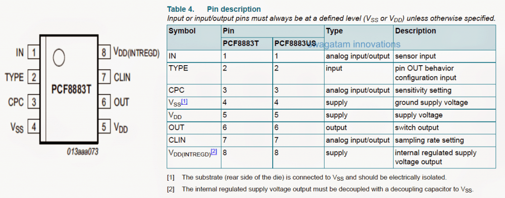
Pinout Details of the IC PCF8883
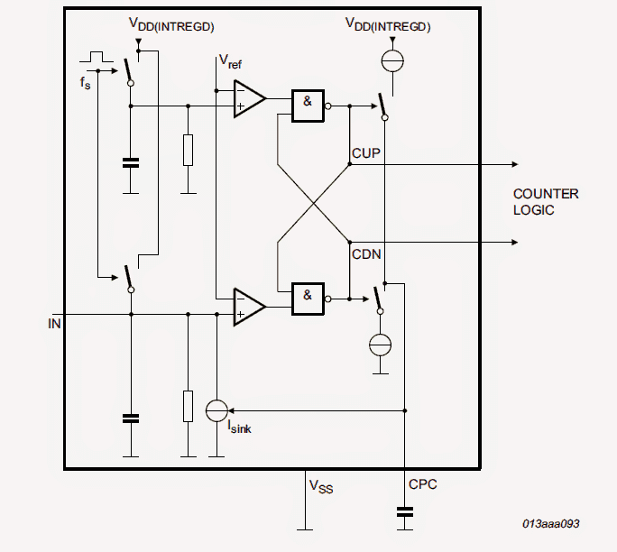
The pinout IN which is supposed to be connected with the external capacitive sensing foil is linked with the ICs internal RC network.
The discharge time given by "tdch" of the RC network is compared by the discharge time of the second in-bult RC network denoted as "tdchimo".
The two RC networks go through periodic charging by VDD(INTREGD) through a couple of identical and synchronized switch networks, and subsequently discharged with the help of a resistor to Vss or the ground
The rate at which this charge discharge is executed is regulated by a sampling rate denoted by "fs".
In case if the potential difference is seen to be dropping below the internally set reference voltage VM, the corresponding output of the comparator tends to become low.
The logic level which follows the comparators identifies the exact comparator that actually could switch before the other.
And if the upper comparator is identified to have fired first, this results with a pulse being rendered on CUP, whereas if the lower comparator is detected to have switched prior to the upper, then the pulse is enabled at CDN.
The above pulses engage in controlling the charge level over the external capacitor Ccpc associated with pin CPC. When a pulse is generated on CUP, the Ccpc is charged through VDDUNTREGD for a given period of time which triggers a rising potential on Ccpc.
Quite on the same lines, when a pulse is rendered at CDN, the Ccpc gets linked with current sink device to ground which discharges the capacitor causing its potential to collapse.
Whenever the capacitance at pin IN gets higher, it correspondingly increases the discharge time tdch, which causes the voltage across the relevant comparator to fall at a correspondingly longer time.
When this takes place the output of the comparator tends to get low which in turn renders a pulse at CDN forcing the external capacitor CCP to discharge to some smaller degree.
This implies that CUP now generates the majority of the pulses which causes CCP to charge up even more without going through any further steps.
Inspite of this, the automatic voltage controlled calibration feature of the IC which relies on a sink current regulation "ism" associated with pin IN makes an effort to balance out the discharge time tdch by referring it with an internally set discharge time tdcmef.
The voltage across Ccpg is current controlled and becomes responsible for the discharge of the capacitance on IN rather rapidly whenever the potential across CCP is detected to be increasing.
This perfectly balances the increasing capacitance on input pin IN.
This effect give rise to a closed loop tracking system which continuously monitors and engages into an automatic equalizing of the discharge time tdch with reference to tdchlmf.
This helps to correct sluggish variations in capacitance across IN pinout of the IC.
During rapidly charging sates for example when a human finger is approached the sensing foil quickly, the discussed compensation might not transpire, in equilibrium conditions the length of the discharge period do not differ causing the pulse to alternately fluctuate across CUP and CDN.
This further implies that with larger Ccpg values a relatively restricted voltage variation for each pulse may be expected for CUP or CDN.
Therefore the internal current sink gives rise to a slower compensation, thereby enhancing the sensitivity of the sensor.
On the contrary, when CCP experiences a decrease, causes the sensor sensitivity to go down.
In-Built Sensor Monitor
An in-built counter stage monitors the sensor triggers and correspondingly counts the pulses across CUP or CDN, the counter gets reset each time the pulse direction across the CUP to CDN alternates or changes.
The output pin represented as OUT undergoes an activation only when adequate number of pulses across CUP or CDN are detected.
Modest levels of interference or slow interactions across the sensor or input capacitance does not produce any effect on the output triggering.
The chip makes note of several conditions such as unequal charge/discharge patterns so that a confirmed output switching is rendered and spurious detection are eliminated.
Advanced Start-up
The IC includes an advanced start-up circuitry which enables the chip to reach equilibrium rather quickly as soon as the supply to it is switched ON.
Internally the pin OUT is configured as an open drain which initiates the pinout with a high logic (Vdd) with a maximum of 20mA current for an attached load.
In case the output is subjected with loads over 30mA, the supply is instantly disconnected due to the short circuit protection feature which is instantly triggered.
This pinout is also CMOS compatible and therefore becomes appropriate for all CMOS based loads or circuit stages.
As mentioned earlier, the sampling rate parameter "fs" relates itself as 50% of the frequency employed with the RC timing network.
The sampling rate can be set across a predetermined span by appropriately fixing the value of CCLIN.
An internally modulated oscillator frequency at 4% through a pseudo-random-signal inhibits any chance of interferences from surrounding AC frequencies.
Output State Selector Mode
The IC also features a useful "output state selection mode" which can be used for enabling the output pin to either in the monostable or bistable state in response to the capacitive sensing of the input pinout. It's rendered in the following manner:
Mode#1 (TYPE enabled at Vss): The output is rendered active for sp long as the input is held under the external capacitive influence.
Mode#2 (TYPE enabled at VDD/NTRESD): In this mode the output is alternately switched ON and OFF (high and low) in response to subsequent capacitive interaction across the sensor foil.
Mode#3 (CTYPE enabled between TYPE and VSS): With this condition the output pin is triggered (low) for some predetermined length of time in response to each capacitive sensing inputs, whose duration is proportional to the value of CTYPE and can be varied with a rate of 2.5ms per nF capacitance.
A standard value for CTYPE for getting around a 10ms delay in mode#3 could be 4.7nF, and the maximum permissible value for CTYPE being 470nF, which may result in with a delay of about a second.
Any abrupt capacitive interventions or influences during this period are simply ignored.
How to Use the Circuit
In the following sections I have explained a typical circuit configuration using the same IC which can be applied in all products requiring precision remote proximity stimulated operations.
The proposed capacitive proximity sensor may be diversely used in many different applications as indicated in the following data:


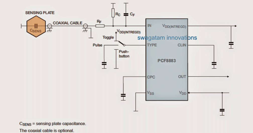
A typical application configuration using the IC can be witnessed below:
Application Circuit Configuration
The + input supply is attached with the VDD. A smoothing capacitor may be preferably connected across and VDD and ground and also across VDDUNTREGD and ground for more reliable working of the chip.
The capacitance value of COLIN as produced on pin CLIN fixes the sampling rate effectively.
Increasing sampling rate may enable enhance reaction time on the sensing input with a proportionate increase in the current consumption
Proximity Sensor Plate
The sensing capacitive sensing plate could be in the form of a miniature metal foil or plate shielded and isolated with a non conductive layer.
This sensing area could be either terminated over a longer distances via a coaxial cable CCABLE whose other ends may be linked with the IN of the IC, or the plate could be simply directly connected with the INpinout of the IC depending on the application needs.
The IC is equipped with an internal low pass filter circuitry which helps to suppress all forms of RF interferences that may try to make way in to the IC through the IN pin of the IC.
Additionally as indicated in the diagram one may also add an external configuration using RF and CF to further enhance the RF suppression and reinforce RF immunity for the circuit.
In order to achieve an optimal performance from the circuit, it's recommended that the sum of the capacitance values of CSENSE + CCABLE + Cp should be within a given appropriate range, a good level could be around 30pF.
This helps the control loop to work in a better way with the static capacitance over CSENSE for equalizing the rather slower interactions on the sensing capacitive plate.
Achieve Increased Capacitive Inputs
For achieving an increased levels of capacitive inputs it may be recommended to include a supplementary resistor Rc as indicated in the diagram which helps to control the discharge time as per the internal timing requirement specs.
The cross sectional area of the attached sensing plate or a sensing foil becomes directly proportional to the sensitivity of the circuit, in conjunction with the value of the capacitor Ccpc, reducing Ccpc value can greatly affect the sensitivity of the sensing plate.
Therefore for achieving an effective amount of sensitivity, Ccpc could be increased optimally and accordingly.
The pinout marked CPC is internally attributed with a high impedance and therefore could be susceptible to leakage currents.
Make sure that Ccpc is chosen with a high quality PPC of MKT type of capacitor or X7R type for obtaining optimal performance from the design.
Operating at Low Temperatures
In case the system is intended to be operated with a restricted input capacitance of upto 35pF and at freezing temperatures -20 degrees C, then it may be advisable to bring down the supply voltage to the IC to around 2.8V.
This in turn brings down the operating range of Vlicpc voltage whose specification lies between 0.6V to VDD - 0.3V.
Moreover, lowering the operating range of Vucpc could result in lowering the input capacitance range of the circuit proportionately.
Also, one may notice that as Vucpc value increases with decreasing temperatures as demonstrated in the diagrams, which tells us why appropriately lowering the supply voltage helps in decreasing temperatures.
Recommended Component Specifications
Table 6 and Table7 indicates the recommended range of the components values which may be appropriately chosen as per the desired application specifications with reference to the above instructions.
Reference: https://www.nxp.com/docs/en/data-sheet/PCF8883.pdf


Questions & Answers
Which circuit would work best as a proximity detector? I want to be able to detect when possible robbers come near my vehicle when it is parked. I would vary the sensitivity so I could detect when someone touches my vehicle or if someone is close to it.
The above deigns won’t work well for automobile applications, instead I would recommend using a PIR based deign as explained in the following post:
https://www.homemade-circuits.com/pir-burglar-alarm-circuit/
Hi Swagatam. I want to build a non-contact capacitive level sensor circuit for car coolant water bottle. After viewing the above circuits and reading comments it seems none will work. I just need it to activate a LED when water runs low (emptys) in coolant bottle. I do not want to drill/cut the bottle as I am afraid the bottle will leak with time due to expansion/contraction. Do you have any ideas? Thanks
Hi Michael, yes capacitive sensors cannot detect fluid, they can only detect RF radiating sources.
Is your coolant water bottle completely opaque, or can some light pass through it?
If light can pass, then perhaps we can configure an LED/LDR based sensor to detect a specific water level in the bottle.
I cannot see any other easy way to accomplish this.
Hi Swagatam, thank you very much for your post. I have built circuit #3 with a different MOSFET (IRF540 instead of IRF511). The buzzer is always on, no matter how I regulate the potentiometer, or if I am touching the plate or not. I checked for errors in my connections, but everything looks ok. Is this problem only caused by the component substitution? Thanks
Hi Anton,
Looking at the MOSFET circuit I can see that its gate is connected to the positive line via the 100 Meg and 100k resistors.
That means the MOSFET would remain switched ON always when powered, which is wrong according to me.
Please disconnect the 100k preset end from the positive supply and connect it with the ground of the circuit.
Now check the response.
Yes, that was the problem, thank you. With your suggested change the circuit is now working. Nevertheless, it is not possible to adjust the sensibility. I’ve found that if I connect instead one end of the potentiometer to the positive supply and the other to the ground the sensibility can be changed ((I suppose this works by varying the reference voltage at the gate). Maybe the schematic was just missing a ground connection at the opposite (left) side of the pot. Tried to send you some other observations by email
I saw your email, thanks for illustrating the three versions, as given below:
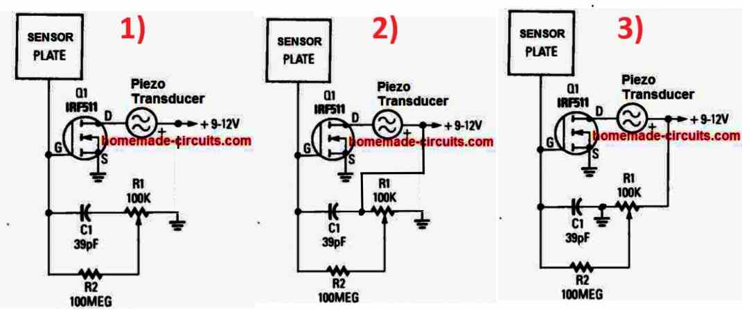
Now we know that the circuits and schematics published in magazines can never be trusted.
I think the 3rd design makes more sense if it allows you to modify the sensitivity of the MOSFET.
In this design the capacitor is connected across gate/ground which looks more logical because here the capacitor acts like a filter, preventing high frequency noise from disturbing the MOSFET and keeping the buzzer silent unless a real human proximity is detected.
So according to me the role of the capacitor is just to prevent false triggering of the MOSFET due to external RF noise.
Thanks a lot! I have another question: is there any way to modify the circuit to increase the sensibility? I am now using a 20 cm diameter metal plate; at maximum sensibility, my hand starts to be detected only at a distance of roughly 2 cm. (I also plan to try circuit #4, which is oscillator-based)
The easiest way to increase is sensitivity is by removing the preset and the capacitor, and connecting the 100M resistor between the MOSFET gate and ground.
So basically the MOSFET will have only two things, one 100M resistor across gate and ground, and a touch plate attached with the gate.
Ok, thanks. I’ll try
Hi Swagatam, I am interested in modifying the same #3 circuit to use it as a sensor for Arduino. In order to do that, I should get from it a variable voltage output (between 0 and 5 volts). I can’t figure out how to do it, also because the circuit works at a higher voltage than the Arduino. Can you give me some suggestion about that? Thanks in advance.
Hi Anton, to make the circuit#3 work with 3V or 5v supplies, you can replace the MOSFET with a Darlington BJT such as C547.

Or you can try the following design:
Can aluminum foil be used as a touch medium? If so, what are the parameters for size? I am particularly interested in the mosfet design and want to detect animals climbing a pole to steal food from a bird feeder.
Yes, aluminum will also work, in fact any metal will work as the detector plate.
The size should be minimum 3 x 3 inches.
However, I would recommend a PIR circuit instead, for a foolproof working, such as this one:
https://www.homemade-circuits.com/pir-burglar-alarm-circuit/
we need photo electric sensro in diffused type
Sorry, I don’t have a circuit based on photoelectric sensor.
how we can simulate the circuit
how to get sense plate?
No need to simulate, you can build it practically, it will work. For the sensor you can use any small steel plate utensil.
if we want to have simulation result of it
how can consider the sense pad? in simulation tool like spice model
The sense pad imitates a capacitive touch sensor, I am not sure what this would be like in your spice model.
can i use this circuit for monitoring sludge in water tank as sludge increase from threshold then ill get alarm
I don’t the above circuits would be able to detect sludge in water tank, these circuits are designed only to detect human presence near the sensor.
Hello Swagatam
I have a question?
Proximity alarm capacitive sensor circuit for a vehicle body, second circuit.
https://www.homemade-circuits.com/precision-capacitive-touchproximity/
I recreated the circuit and it works perfectly with an external battery! But only outside of my Toyota C-HR 1.8 Hybrid. If I put the circuit in the trunk, nothing works anymore.
What can I do that it also works in the trunk
The circuit as a proximity alarm safety system for a vehicle body.
Do you have any tips for that?
Hello Helmut, Glad you could recreate the circuit successfully, however it won’t work inside a car trunk, because the car body acts like a shield and a massive ground, so it will not allow the sensor plate to sense a human body even if its too close to it.
Hi,
how can I use thias circuit to get analogue output corresponding to the sensing distance.
please guide.
thanks
deepak
Hi,
You can get an analogue output on pin#3 of the IC, and source pin of the FET
Hello Swagatam,
Can you suggest a circuit of dielectric type capacitive proximity sensor that can detect both conductive and non-conductive objects?
Hello Abhay, Can you explain the functioning of dielectric type capacitive proximity sensor, I have not yet investigated this concept.
In the circuit using IC 741, I want to turn on the relay until I touch or place hand near the touch plate and turn off if my hand move away from touch plate. I mean always on if my body touch or is near the touch plate and off if my body move away from touch plate. Is it possible with the circuit you wrote above? I tried to use TTP223 capacitive touch sensor but it was turned off after about 5 seconds itself. If there are any sensor kit similar functions like I want please recommend me^
thank you from South Korea~
I think that may be possible using the first circuit, since our body acts like a large 50/60Hz hum source, this can be used to activate/deactivate the mentioned circuit.
Thank you Sir, I will buy some components and try the circuit^. I will let you know the result^
Take care~
Sure, no problem…
Hey!
When the MTCH101 microcircuit is turned on, the supply voltage is turned on, and the simultaneous touch occurs
– Automatic Environmental Compensation
chip.
You can advise an analog of MTCH101
without, where not – Automatic Environmental Compensation
chip? Desirable SOT23-6 with sensitivity adjustment
Language translation. Google translate /
sorry, I have no idea about it!
Hello Swagatam,
I built the first circuit (the one with IC 741) and I couldn’t get it to work. I am using the bottom of a Sprite can as the touch-place. For C1, I have polarized and unpolarized 1μF capacitors, which one should I use? For Q1, I am using NTE312 JFET transistor instead of your suggested 2N3819. For the op-amp, I am using NTE941M & NTE941SM IC Op-amp instead of your suggested IC 741. For the PNP transistor, I am using NTE159 instead of your suggested BC557. Could you have any suggestion on what changes should I make to make this circuit work ? I can send a picture of what I have to hitman2008@live.in if it is still active.
Thank you
Hello Mustfa,
Since you have used different FET and op amp it will be difficult to judge about their working without testing them practically.
Basically you have to first confirm the stages separately through the following tests:
1) Manually short circuit the D/S pins of the FET and check whether the op amp toggles ON, and the red LED lights up or not. Removing the short must switch OFF the op amp output.
2) manually connect the gate of the FET directly with the positive line, and check for the same response as above.
3) when you touch the touch plate, confirm using a meter whether it causes a drop in voltage across pin3 and ground?
4) Connect a 470uF capacitor directly in parallel to the relay coil to ensure it switches ON/OFF without stuttering.
5) The 1uF capacitor can be any capacitor, polarity does not matter
Thank you for your quick response.
Will the 2nd circuit work for my motorcycle if i connect the cable for the plate to the body?
Won’t this be as if i am connecting it to the -12v supply or 0 supply?
Will it behave as a plate or it will cancel it?
I used this module TTP223 Touch button Module and connected to body but it doesn’t work.
For the second circuit, you cannot connect the touch plate to the body of the motorcycle. The touch plate should be isolated from the body and should not be too big. It could be a 6 square inch plate maximum or smaller
The sensing plate can be built using any metallic plate, no special modules are required.
In the second circuit what are the values for R8 and R9?
You can use 10k for both