If you are having difficulty in understanding how to use an LM3915 IC, this article will help you to easily construct any desired applicable circuit using this IC. Here, I will elucidate the datasheet of the IC LM3915, its pinout functions, its main electrical specifications, and also a few useful application circuits.
General Description
The LM3915 is a monolytthic IC designed to sense analogue voltage signals, and produce an incremental or sequential logic switching across its 10 output.
Inidicating devices likes LEDs, LCD or vaccum displays can be attached with these outputs to obtain a corresponding visual indication in response to the varying input analogue signal.
The IC has one pinout for designating whether the output LEDs will sequence individually (dot mode) or in form of a bar graph.
The LED can be connected without limiting resistors since the IC includes internal programmable current regulation for the 10 outputs.
The IC circuit including all the 10 LEDs can be operated using as low as 3V supply and upto 25V.
The IC features an adaptable voltage reference and a precise 10 step voltage divider. The high-impedance input buffer can be fed with analogue voltages from 0V to within +1.5V.
Further more, the inputs are well protected against signals upto the range of ±35V.
The input buffer runs 10 opamp comparators which are all referenced to the precision divider network. Accuracy level of the system is normally in the vicinity of 1 dB.
The LM3915’s 3 dB/step display is built for accepting input signals with broad dynamic range. For example the input can be in the form of audio or music signal, varying light intensity or vibrational electricity.
Audio applications could be in the form of average or peak level indicators, power meters and RF signal strength meters.
Upgrading traditional analogue VU meters with an LM3915 based LED bar graph gives a better illuminated response, a durable display with improved field of vision enabling better interpretation of input signal.
The LM3915 is very simple to use. In addition to the ten LEDs you can even use a 1.2V full-scale-deflection meter with just one resistor.
Another separate resistor sets up the full-scale range between 1.2V to 12V regardless of supply voltage value. The brightness of the LED is easily controllable with a single external pot.
Typical LM3915 Circuit Configuration
The following image shows how the IC LM3915 can be setup in its most typical or basic functional mode.
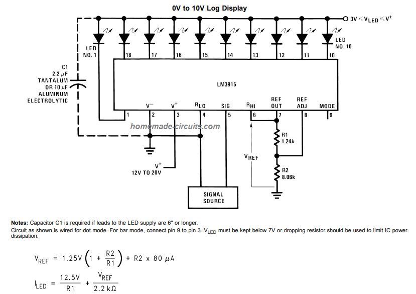
If you are a new hobbyists and want to configure the pinouts of IC LM3915 or LM3914 quickly to get the required actions, then the following diagram could be used. The pinout details are I have explained below:
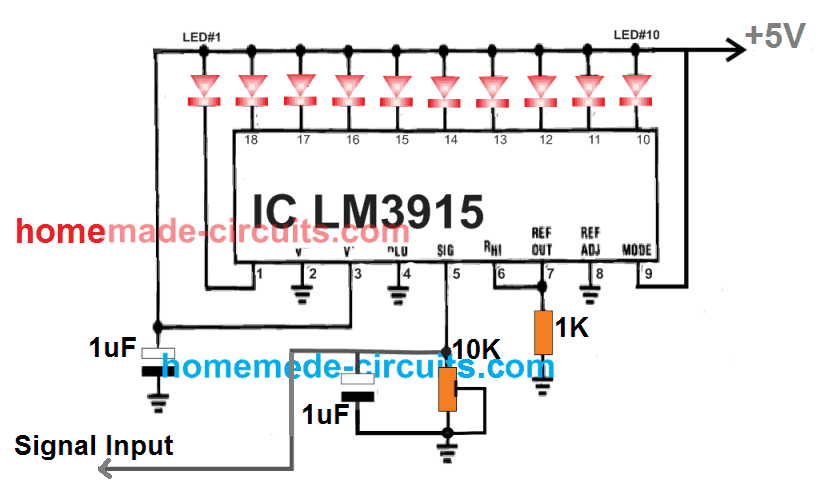
pin#10, pin#11, pin#12, pin#13, pin#14, pin#15, pin#16, pin#17, pin#18, and pin#1 = All are outputs for LED connection. LEDs do not need an external resistance, but preferably the LED supply line must be restricted to 5V to keep the dissipation on the lower side.
Pin#3 is the VDD or the positive supply input for the IC, which can take any supply between 3V and 25V, but I recommend using 5V to keep the LED dissipation on the lower side.
Pin#8 is the Vss or the ground (negative) supply pin of the IC.
Pin#6 and pin#7 can be joined together and terminated to ground line via a 1K resistor.
Pin#5 must be configured as shown in the above diagram through a 10k preset and a capacitor. This preset can be adjusted for setting the full scale LED illumination range depending on the strength of the input signal.
Pin#9 could be left unconnected (open) or connected to the +supply line. When left unconnected, the LEDs sequence up/down individually appearing like a running "DOT" and hence called the DOT mode. When pin#9 is connected to the positive line, the LED sequence like a up/down moving illuminated bar, hence called the bar mode.
Once this is done, it's just about feeding the input signal and watch the wonderful movement of the LEDs as per the varying input signal or music amplitudes
Absolute Maximum Ratings
The absolute maximum rating of LM3915 indicates the maximum voltage and current parameters the device is permitted to handle.
- Supply Voltage = 25V
- Output Supply on the LEDs if you are using a separate supply here = 25V (same as above)
- Maximum Input Signal Range = +/-35V
- Divider Reference Voltage = -100mV to Supply Level.
- Power Dissipation = 1365 mW
Internal Layout of the IC
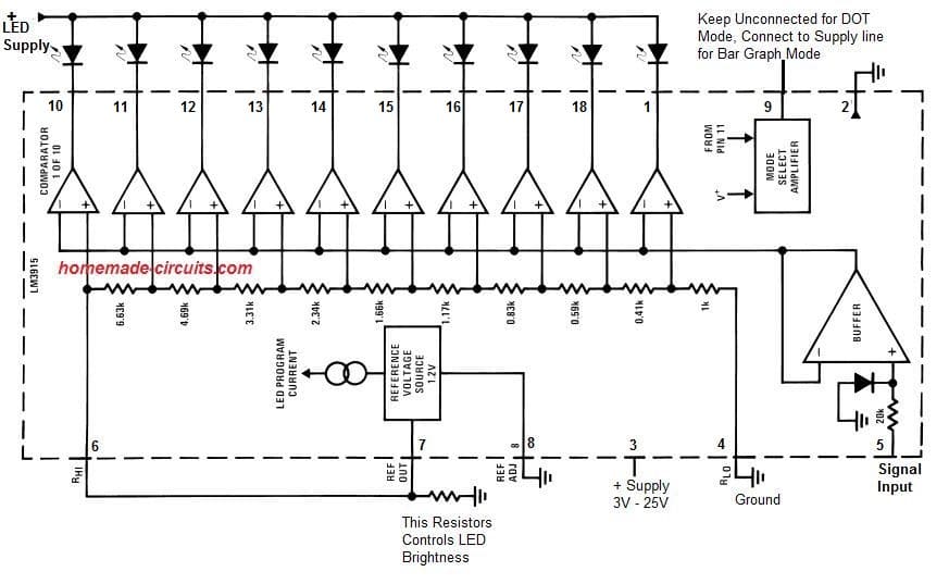
The following diagram shows the internal layout of the IC. We can see how the opam comparators are arranged for processing the input signal at pin#5. The reference at pin#7 applied in an incremental order across the opamp non-inverting inputs through a ladder type resistor divider network.
Functional Description
The above basic LM3915 block diagram provides the general perception of the circuit’s functioning. A high input impedance voltage follower buffer responds to the input pin#5 signals.
This pinout is secured against over-voltage and reverse polarity signals. The signal from buffer then goes to a group of 10 comparators.
Each of this opamps are biased to an incrementing reference levels through the resistor divider series. In the image above, the resistor network is linked with the internal 1.25V reference voltage.
Here, , for every 3 dB rise in the input signal, a switch in the comparator level is triggered causing the respective LED to move and sequence accordingly, interpreting the signal response.
This internal resistor divider could be operated with potential of 0 - 2 volts at pin#5, through an external resistive divider network.
INTERNAL VOLTAGE REFERENCE
The reference voltage for the IC LM3915 is intended to be variable so that it builds up a tiny 1.25V across REF OUT (pin #7) and REF ADJ (pin #8).
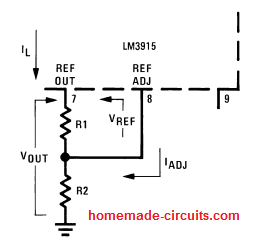
The reference voltage is implemented across the resistor R1 which can be changed as per preference. Because we have a constant supply DC voltage, a constant current I1 is allowed to move through the output setting resistor R2 enabling an output voltage of:
VOUT = VREF (1 + R2/R1) + IADJ R2
The current taken in by the reference voltage pin #7 decides the amount of LED current. We can expect around 10 times this current that may be permissible to be consumed by each illuminated output LED.
This current is more or less constant regardless of supply voltage variations and temperature changes. Current used by the internal 10-resistor divider, and the external current and voltage-setting divider must be taken into account while calculating LED drive current.
The IC provides a feature for modulating real time referenced LED brightness, or in response to input voltage variations and other signals. This allows inclusion of many innovative displays or options for producing input over-voltages, alarms, etc.
The outputs of LM3915 are all internally current controlled NPN BJT buffers as shown below.
An internal feedback hook restricts the transistor from over current situations. Output current for the LEDs is fixed at roughly to 10 times the reference load current, irrespective of variations in the output voltage until of course the transistors are not saturated with high input supply.
How to Use the MODE Pin #9
This pin is configured to enforce two functions. Please see the following simplified block diagram.
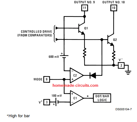
DOT OR BAR MODE SELECTION
When the pin #9 is connected to the + supply line (or between -100mV and supply level), the comparator C1 senses this, and sets the output in the bar graph mode. In this mode all the LEDs respond in an illuminated "bar" like fashion which moves up/down in response to the varying signals at pin #5.
If the pin #9 is unconnected, the outputs are set in the "DOT" mode. Meaning the LEDs sequence up/down individually one at a time, producing a pulsating illuminated DOT or point like appearance.
The basic way to configure pin #9 is either keep it open or unconnected for implementing dot mode or connect it to supply V+ for implementing the bar mode.
In bar mode operation, pin #9 should be hooked up straight away with pin #3. The LED + line that supplies large currents to the LED chain should not be used with pin #9 so that large IR drops is kept aloof from this pin.
To ensure that the output LED display works correctly when more than one LM3915s are cascaded in dot mode, special circuitry in built-in such that the LED at pin #10 shuts off for the first LM3915 IC at the momenet when LED #1 of the second LM3915 is switched ON.
The design for cascading LM3915 ICs together in dot mode can be witnessed below.
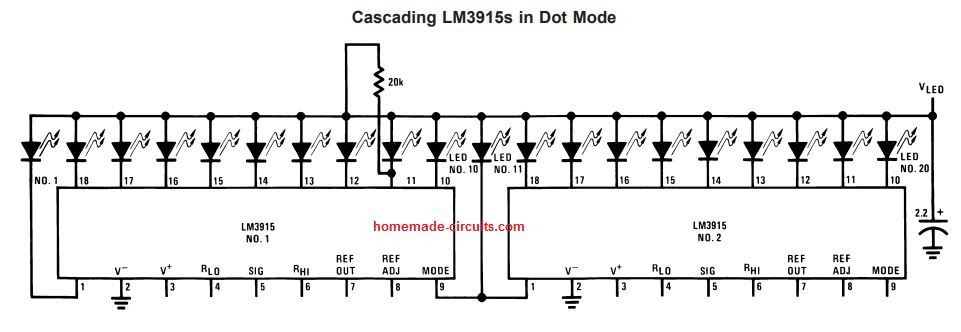
With the condition that the input signal voltage is below the threshold of the second LM3915, LED #11 stays switched off. Pin #9 of the first LM3915 hence experiences an effective open circuit which causes the IC to run in dot mode.
However the moment the input signal crosses over the threshold of LED #11, pin #9 of the first LM3915 is dropped by a level equal to the LED's forward voltage (1.5V or more) below VLED.
This situation is instantly picked up by comparator C2, referenced 0.6 V below VLED. It compels C2 output to go low, shutting off output transistor Q2, subsequently switching OFF LED #10.
VLED is detected through the resistor 20k attached to pin #11. The tiny current (under 100 µA) which is redirected from LED #9 does not produce any recognizable effect on the intensity of the LED. An additional current source at pin #1 maintains a minimum of 100 µA running through LED #11 regardless of whether or not the input signal rise is enough to switch OFF the LED.
This means that pin #9 of the first LM3915 is kept sufficiently low such that it keeps LED #10 shut off while any of the upper LEDs in the sequence is illuminated.
Although 100 µA doesn't usually create considerable LED brightness, it might be visible just enough if high-efficiency LEDs are employed and in total darkness. If this sounds unacceptable, the easy remedy would be to shunt LED #11 with a 10k resistor.
The 1V IR drop is higher than the minimum 900 mV necessary to maintain LED #10 switched OFF, but small enough ensuring that the LED #11 does not conduct over undesired limits.
The most challenging issue arises when substantial LED currents happen to be consumed, specifically in bar graph mode.
Such currents moving away from the ground pin lead to voltage drops within outer wiring, causing glitches and fluctuations.
Getting the returning cables from signal ports, ground references and from bottom-side of the resistor chain to a single common terminal that may be closest to pin #2 becomes an ideal approach.
Extended wire connections from VLED towards the common LED anodes may trigger oscillations. Based on how serious the issue is a 0.05 µF to 2.2 µF decoupling capacitors can be used between LED anode common and pin #2.
This helps to dampen any developed oscillations. If LED anode supply line wiring is unreachable, identical decoupling across pin #1 to pin #2 proves just adequate for cancelling the interference.
Power Dissipation
Power dissipation, specifically in bar mode needs to be taken into account. For instance, with a 5V supply and all LEDs set up to work with 20 mA current, the LED driver section of the IC can be expected to dissipate over 600 mW.
In cases like this a 7.5Ω resistor can be used in series with the LED supply line, which might help to bring down the dissipation level to half the original value. The negative end of this resistor must be reinforced with a 2.2 µF solid tantalum bypass capacitor with pin #2.
CASCADING LM3915 ICs
For using display signals of 60 dB or 90 dB dynamic range, you may require a few LM3915 ICs to be cascaded together.
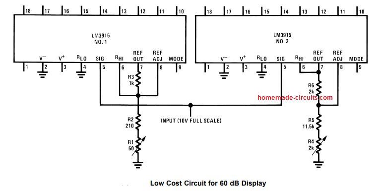
A straightforward, affordable method of cascading a couple of LM3915s would be to fix the reference voltages of the two ICs 30 dB apart as indicated in the .
Potentiometer R1 is employed to regulate the full scale voltage of the first LM3915 IC to 316 mV marginally while the second IC’s reference is scheduled at 10V by R4.
The disadvantage of this technique is that the switch ON threshold of LED #1 is merely 14 mV and, considering that the LM3915 may have an offset voltage of up to 10 mV, substantial errors can take place.
This method is absolutely not advised for 60 dB displays necessitating decent precision at the few initial display thresholds.
A superior technique shown in the below figure keeps the reference at 10V for each of the two LM3915 ICs and boosts the input signal to the lower LM3915 by 30 dB. Given that a pair of 1% resistors are able to fix the amplifier gain at ±0.2 dB, the need for a gain reduction becomes unnecessary.
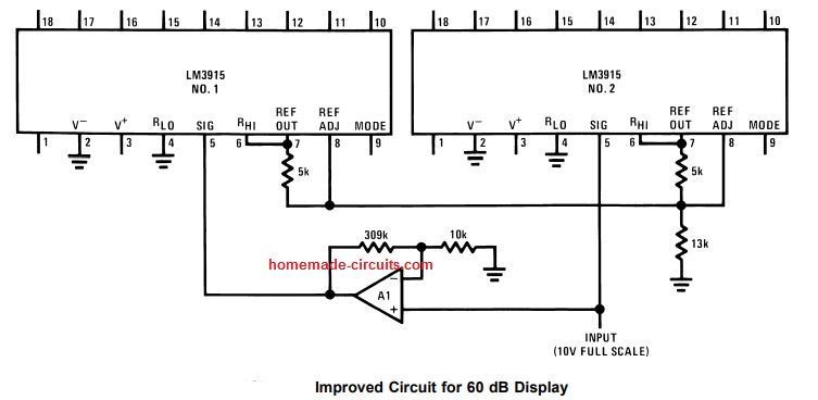
However, an 5 mV opamp offset voltage might be able to alter the first LED switching limit by around 4 dB, which necessitates an offset trimming.
Remember that just one adjustment may help to nullify the offset across the two the precision rectifier along with the 30 dB gain stage.
On the other hand, rather than amplifying, input signals of reasonably high amplitude could be supplied right to the lower LM3915 and subsequently attenuated by 30 dB to push the 2nd LM3915 IC.
LM3915 Application Circuits
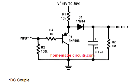
Half-Wave Peak Detector
The best way to exhibit an AC signal through IC LM3915 is to implement it directly to pin 5 unrectified. Because the LED illuminated signifies the instantaneous magnitude of the applied AC waveform, it becomes possible to determine both maximum and average values of audio signals in the same method.
The LM3915 responds well to positive half-cycles specifically but will not be harmed any input signals as much as ±35V (or even way up to ±100V if a 39k resistor is used series with the input signal).
It's advised that you operate the circuit in the DOT mode and allow each LED to draw 30mA in order to get optimum brightness from the set up.
In order to detect mean value of the AC or for peak detection, rectification of the signal will be required.
If an LM3915 is setup with 10V full scale across its voltage divider, the switching threshold for the first LED will be just 450 mV. An ordinary silicon diode rectifier might not work effectively at the lower levels because of the 0.6 V diode threshold.
The half-wave peak detector in the above Figure employs a PNP emitter-follower ahead of the diode. Due to the fact that the transistor’s base-emitter voltage blocks the diode offset in the range of around 100 mV, the method works good enough with single LM3915 applications using a 30 dB display.
More Application Circuits
There are actually a huge number of circuit applications which you can build using the IC LM3915. I have already discussed a a handful of them in this website, which you can refer by visiting HERE:
So folks this was a short description explaining the datasheet and pinout details of the IC LM3915. If you have any further doubts please let us know through the comment box below, we'll try to get in touch at an earliest.
References
https://www.digchip.com/datasheets/download_datasheet.php?id=514550&part-number=LM3915


Comments
Hello,
I’m building a 10 band audio spectrum analyzer using 10x LM3915 ICs. I have a pretty stable circuit but I want to improve on it where I can. I am aiming for a ‘fast attack, slower decay’ for the bargraphs. I currently have a 2.2uF cap and a 18k resistor in parallel from the BAT85 rectifier to ground, with the diode/cap/resistor node to pin 5. Is it just a case of adjusting the cap and resistor to change the attack/decay?
Also, I want to add the feature of a 20 bar led by using a second LM3915. How do i go about connecting this? With this, at the moment ICA, lets say, pin 4 is GND, Pin 6&7 are connected to a 680R to GND. DO i lift pin 4 on ICA and connect to pin 6 on ICB?
Hope you can help.
Thanks
Please ignore the previous diagram link which I sent you, here’s the corrected one with a 1N4148 diode included, which is crucial for implementing the fast attack and slow decay perfectly…
https://www.homemade-circuits.com/wp-content/uploads/2025/11/LED-slow-decay-fast-attack-circuit.jpg
Hi, to get fast attack and slow decay, can you please try the following configuration for each LED:
https://www.homemade-circuits.com/wp-content/uploads/2025/11/LED-slow-decay-fast-attack.jpg
For cascading two IC LM3915s, I think you can do something as done in the first diagram of this article…let me know if you have any further doubts…
https://www.homemade-circuits.com/how-to-make-simple-vu-meter-circuit-at/
Hi Mr. Swagatam;
Is it possible to unite the above circuit and the auidible battery test circuit? After your confirmation I will supply the LM3915 and try it.
Hi Suat, yes it is possible, however, first I would suggest you to confirm the battery tester circuit, whether it actually works as per our expectations or not…if it works then I can definitely show you how to integrate it with the above LM3915 design…
Yes Swagatam it works and fine since I have tested it yesterday. For instant I can hear weak sound for the 1,5V batteries and beeps louder for the 9V batteries.
I would like to use it fixed for the 12V batteries and 3 leds are enough for me. The leds will resemble the a) low / bad b) medium and c) good / full.
Ok, that’s great, Suat.
However, integrating it directly with an LM3915 LED driver can be difficult, so you may have use the LM3915 to detect the sound level from the speaker of the battery tester, using the following circuit:
https://www.homemade-circuits.com/wireless-music-level-indicator/
Thank you for recommending that 2n2907 transistor, is it ok to use a 1k resistor from the output pin of the Lm 3915 going towards the base of transistor, power with a regulated 12 volt dc supply and use a 200 ohm resistor in series with the lazer diode, as you can desern, I am still learning, if this can workout I will be so very happy.
Regards donald
Yes 1K resistor can be used for the bases of the transistor. 12V can be used for the LM3915 circuit, but the lasers connected across the collector of the transistors must be supplied with a 3V stabilized DC, to safeguard the lasers.
Hi
Thank you so much for getting back to me, I do appreciate it, I am working on a vu meter circuit utilizing the same lm3915 chip and would
like to replace the leds with lazer dot diodes, The lazers are the cheap ones 780nm (3 mw) runs with 3 volt dc and working current < 100ma, was planning to use maybe a resistor just after the output pin then 2n3906 pnp transistor if this transistor is not suitable, can you suggest a replacement from there am totally lost, Can you help?
Regards donald
Hi, yes your thinking is correct, you can use PNP transistor driver for driver the lasers, but instead of 2n3906, I would recommend using 2N2907 transistor.
And also make sure to operate the circuit with a regulated and fixed 3V DC source so that the lasers do not burn.
Thanks!
Does the signal to LM3915 have to be audio or can it be voltage from a battery? How can I make the LED’s light based on voltage input from a battery?
Audio is also a voltage. so Yes battery voltage can be used with LM3915 for detecting its level.
The IC outputs are designed to go low from 1st pin to the 10th pin sequentially in response to voltages between 0 and 200 mV at pin#5.
So you will have to use a potential divider across pin#5 which can reduce the input voltage range to a max of 200 mV, so that you can get the proportionate readings on the IC output
sir,
please provide a pcb layout for a singe lm 3915 audio level indicator
Dear Mr. Swagatam. Is the scheme powered by 12v from the battery and at pin 5 with 15 …….. 26v from a wind turbine (ie separately from the 12v power supply)?
I tried an MPPT scheme, but I burn the transistor Bc547 (which supplies + LEDs), the one with zener diode 6V and with Lm 3915 which commands 10 IRFZ 44.
What can you recommend? Once again I thank you from the heart and I hope you can help me.
Dear Marian, The IC output side LED line must be supplied with 5V, the Vcc pin of the IC can work with up to 30 V. Pin5 needs only a 0.2V range to process…so the input supply must be reduced to this range using resistive divider….such as a 10K preset, whose center pin can be fed to the input signal via another 10 K resistor
Mr Swagatam. can I do a controller with LM3915 if at the 5 pin I have an input of 5 – 26V separated from the supply voltage? That’s to make a wind controller.
Thanks a lot for the answer.
Hi Marain, yes that’s quite possible
Sir, Can I use LM 3914 in place of LM3915, because LM 3915 is not available in our locality.
yes you can use it!