IC 4049 is a CMOS hex inverting buffer IC that has six independent inverters or NOT gates. It is commonly used in various electronic circuits such as oscillators, timers, and voltage regulators. Here's the datasheet for IC 4049:
General Information:
- Manufacturer: Multiple
- Product Category: Buffers & Line Drivers
- RoHS: Yes
- Package / Case: PDIP-16
- Logic Family: 4000
- Logic Type: CMOS
- Number of Channels: 6
- Polarity: Inverting Supply Voltage (Max): 18 V
- Supply Voltage (Min): 3 V
- Maximum Operating Temperature: 85 C
- Minimum Operating Temperature: -40 C
Electrical Characteristics:
- Supply Voltage Range: 3V - 18V
- Input Voltage Range: -0.5V to VDD +0.5V DC
- Input Diode Current: +/-10mA DC
- Output Diode Current: +/-10mA
- Output Short-Circuit Duration: Indefinite
- Input Rise and Fall Time: 100ns (max)
- Propagation Delay Time: 100ns (max)
- Quiescent Supply Current: 1uA (max)
- Static Input Capacitance: 5pF
- Dynamic Input Capacitance: 50pF
- Static Output Capacitance: 15pF
- Dynamic Output Capacitance: 50pF
Pinout Configuration:
The pinouts details for the IC 4049 is provided in the following diagram:
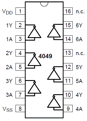
How the Pinouts Work
As shown in the diagram, the pin#1 of the IC is the positive supply input, which must not be exceeded beyond 18 V.
Pin#8 is the ground supply input pin or the 0V supply pin of the IC.
The IC 4049 has 6 independent NOT gates. The triangle shaped figures shown in the above diagram symbolizes the 6 NOT gates of the IC. Each of these NOT gates have 1 input and one output. The tapering side of the triangles with a small circle indicates the outputs of these gates, while the opposite sides indicate the input of the gate.
What does the NOT gate do? NOT gates are basically signal inverters. It is used to invert a given logic signal. The logic signal can be any DC voltage between 3 V and the maximum VDD which is supplied value at pin#1.
Let's take the example of the first NOT gate connected across pin#2 and pin#3 of the IC. If a positive voltage, let's say a +5V is applied to the input side pin#3 of this gate, it will invert the signal and produce a 0 V at its output pin#2. What happens if 9V is applied at the input? The result will be the same, a 0V will appear at the output pin#2.
Now, suppose a 0V is applied at the input side pin#3, this will again prompt the IC to revert the signal oppositely so that a positive voltage is generated at the output pin#2. This positive voltage will be always equal to the value supplied at the VDD pin of the IC, which is the positive supply input of the IC.
Meaning, whenever a 0V or any voltage below 2 V is applied at the inputs of the NOT gates, the outputs will always generate a potential equal to the VDD value.
The above explained NOT gate pinout functioning is the same for all the 6 gates of the IC.
Note: Pins 13 and 16 are not internally connected and are provided for flexibility in layout.
Truth Table
The truth table for a single inverter (NOT gate) of the IC 4049 is as follows:
| Input | Output |
|---|---|
| 0 | 1 |
| 1 | 0 |
Since the IC 4049 has six independent inverters, we can represent its truth table as six columns, with each column representing the truth table for a single inverter.
| Input A | Output A | Input B | Output B | Input C | Output C |
|---|---|---|---|---|---|
| 0 | 1 | 0 | 1 | 0 | 1 |
| 1 | 0 | 1 | 0 | 1 | 0 |
And so on for the remaining inverters. Each row represents the input and output for all six inverters for a particular combination of inputs.
Applications:
- Oscillators
- Timers
- Voltage regulators
- Digital Logic Circuits
- Power Management
- Audio amplifiers
Making an oscillator circuit with a IC 4049 NOT gate is simple and can be done as shown in the following diagram:
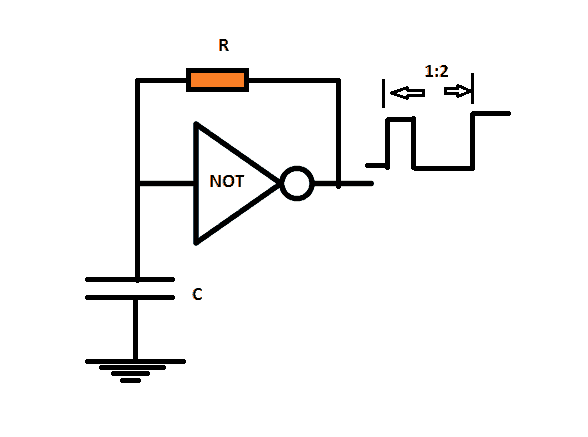
An oscillator is a circuit that produces a repetitive signal without the need for an input signal. A NOT gate oscillator uses a single NOT gate (also known as an inverter) to generate an oscillating output signal.
The formula for a NOT gate oscillator is:
The time period required for each half-cycle will be 1.1 x R x C. This means that the frequency output from a 4049 IC NOT gate oscillator can be expressed as:
f = 1 / 2.2 RC
Transmitter Circuit
A very easy high frequency AM transmitter can be built using a single IC 4049, as demonstrated in the following figure:
Here, the input of the first gate on the left side is connected with the output of the last gate at the extreme right side. This creates a feedback loop causing the all the gates to oscillate at high frequency.
This frequency is transmitted through the antenna of the circuit at pin#10, which can be received through any AM radio receiver.
I have discussed plenty of application circuits using IC 4049 which can be witnessed by visiting the following link:
Need Help? Please Leave a Comment! We value your input—Kindly keep it relevant to the above topic!