This page discusses many types of wideband amplifier circuits. These amplifiers are utilized in a variety of high frequency applications in electronics. We'll talk about how they operate and what makes them unique for specific RF circuit designs.
A wideband amplifier is a circuit that boosts electronic signals over a wide range of frequencies, making it useful for various applications where signals vary in frequency.
Wideband Power Amplifier
This wideband power amplifier doesn't generate a substantial amount of power; it typically operates in the milliwatt range.
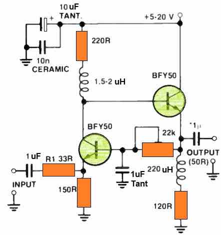
It employs a configuration similar to the common-base/common-collector amplifier but offers power gain, capable of delivering an output ranging from 10 to 180 milliwatts, depending on the power supply voltage.
The common collector stage provides current gain, facilitating power transfer to the load. To achieve the required bandwidth, both stages must operate at relatively high quiescent current levels.
The common-base stage compensates for the input capacitance of the common collector stage, and the inclusion of an RFC (Radio-Frequency Choke) in the emitter of the output device enhances high-frequency response, expanding the amplifier's bandwidth.
R1 can be adjusted to match the input impedance with the source driving impedance.
If needed, two of these amplifiers can be cascaded to produce approximately half a watt output without significant degradation in overall bandwidth.
Adjusting the 1uF capacitors can alter the lower cutoff frequency.
Specifications
Midband power gain ranges from 13 to 15 dB, and the power output is approximately 10 milliwatts with a 5V supply or 180 milliwatts with a 20V supply.
The bandwidth spans approximately 50 kHz to 15 MHz. The input capacitor should be a 50V metallized poly or monobloc type with low inductance.
Wideband Amplifier with DC Feedback
For achieving high and stable gain, a wideband amplifier necessitates multiple stages with various DC feedback paths.
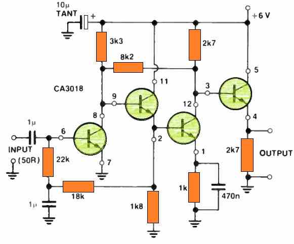
In this configuration, two left-hand and two right-hand transistors form common-emitter/common-collector pairs.
The common collector devices serve as a high-impedance load for the preceding transistor and a low source impedance for the following stage, minimizing internal capacitive feedback.
The circuit employs a CA3018 transistor array IC, and the lower cutoff frequency depends on the capacitor values. It's recommended to use low self-inductance metallized poly capacitors with low voltage ratings.
Specifications
The midband gain is approximately 50 dB, and the bandwidth (-3 dB) extends from 1 kHz to 30 MHz. The maximum input signal should be around 4 mV RMS.
Wideband Cascade Amplifier
The primary characteristic of the wideband cascade amplifier configuration is its ability to isolate the input from the output, resulting in excellent stability regardless of load reactance.
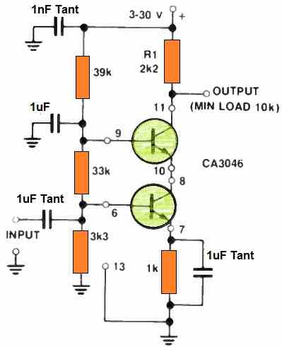
The lower transistor functions as a common-emitter amplifier, while the upper one operates in grounded-base mode.
This setup employs two transistors from a transistor array IC (CA3046), each with an hFE of 110 and a cutoff frequency (f) of 450 MHz.
The upper cutoff frequency is determined by R1, and increasing capacitor values can reduce lower cutoff frequencies. Alternatively, discrete transistors such as 2N706, 2N2369, 2N3607, MPB3646, or 2N5769 can be used.
Specifications
The midband gain (loaded) is approximately 32 dB, and the bandwidth (-3 dB) spans approximately 5 kHz to 4 MHz. It's crucial to ground pin 13 of CA3046 for proper operation.
For the input capacitor, consider using 50V metallized poly types or tag tantalum capacitors (with attention to polarity).
Common Base, Common Collector Wideband Amplifier
This amplifier configuration offers the advantage of low input and output impedances, typically around 100 Ohms.
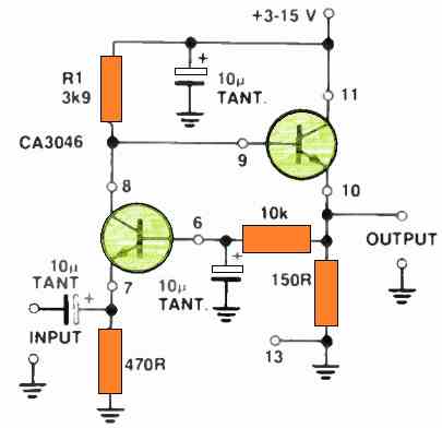
It utilizes two devices from a transistor array IC. For optimal results, use dipped tantalum capacitors and keep lead lengths short.
You can adjust the input impedance to match the source impedance by varying R1, which, in turn, modifies the emitter current of the common base stage.
While this wideband amplifier configuration provides excellent linearity, its gain is not exceptionally high.
Specifications
The midband gain is approximately 17 dB, and the bandwidth (-3 dB) ranges from approximately 150 Hz to 3.5 MHz.
The maximum input at a 5V supply should be around 40 mV RMS, and it's essential to ground pin 13 of CA3046 for proper operation.
Wideband Video Amplifier Circuit
This circuit is an excellent choice for a wideband video amplifier. Its design works with a compound series feedback configuration, which offers several advantages such as high input impedance, low capacitance, and consistent gain across a broad frequency spectrum.
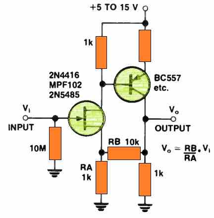
In order to get optimal performance, it may be important to use prefect RF construction practices, according to which the component leads must be kept short and ensure proper bypassing of the power supply.
For effective bypassing, you may want to use both a 100n ceramic capacitor and a 1u tantalum capacitor in parallel.
Please note that both the input and output signals remain in phase in this circuit.
In case you want to adjust the gain, this can be accomplished by varying the value of the 10k feedback resistor.
Wideband RF Amplifier Circuit
This wideband RF amplifier features a bandwidth ranging from approximately 100 kHz to 4 MHz and exhibits high gain and stability.
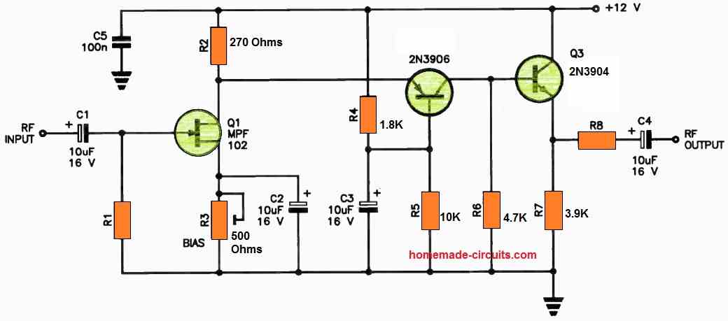
JFET common-source amplifiers are used in the input stage, and Q1 is then directly connected to Q2, a grounded base stage.
A low impedance output is then produced by an emitter follower, Q3.
The grounded base second stage maintains strong stability by offering gain and good input-output separation.
These tantalum-type polarized capacitors are all available. Ceramic should be used for the supply rail bypass capacitor.
The input impedance will depend on the magnitude of R1. This can be set to a small value for sources with low impedance requirements or an increased value, up to a few hundred kilohms, for sources with high impedance requirements.
Similarly, R8 may be chosen to adjust the output impedance. It normally ranges between 39 and 560 Ohms.
R8 might not be included at all if the output connects with a medium to high impedance source.
R3 is tuned to get around 10.5 volts at Q1's drain while the amplifier is initially set up, and it may need to be tweaked a little more for optimal performance afterwards.
Once R3 has been tuned to its ideal value, the trimpot could be replaced by a fixed resistor of an appropriate value. For Q2 and Q3, a large range of transistors are possible.
Wideband Crystal Oscillator Circuit
The following is an universal wideband crystal oscillator with an integrated buffer for parallel resonant crystals.
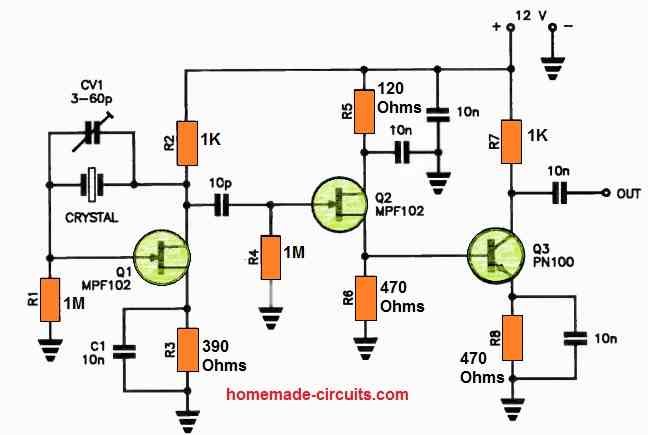
The source-follower Q2, which has a high input impedance and places the least amount of strain on the oscillator stage, receives feedback from the crystal via Q1, whose output is only weakly linked to it through the 10pF capacitor.
Q3 and Q2 are connected directly. Common-emitter amplifier design, with output obtained from the collector through a 10nF capacitor.
When compared to Q1, which is a straightforward periodic oscillator, the Q2-Q3 buffer offers a wideband amplifier with modest gain.
Any source between roughly 7 V and 15 V can be used to power it.
Use of a regulated supply will result in the highest level of stability and minimal output noise.
Wideband Buffer Circuit
The following design works well as a wideband buffer for RF oscillators ranging in frequency from 100 kHz to 20 or 30 MHz.
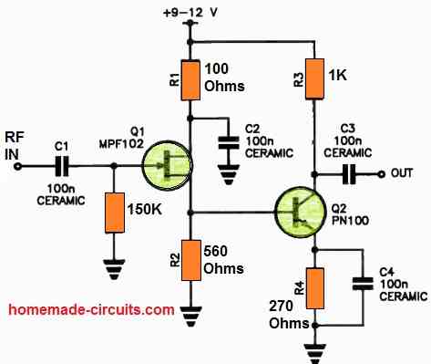
It displays a high input impedance and a relatively low output impedance, has a tiny amount of gain, and is extremely stable.
It also works well as an impedance step-down circuit.
A JFET called Q1 is used as a source-follower. With its output coming from the collector, Q2 is directly linked to it and used as a common-emitter amplifier.
For the highest RF efficiency, ceramic capacitors are always selected because of their small self-inductance.
Wideband TV Signal Booster Circuit
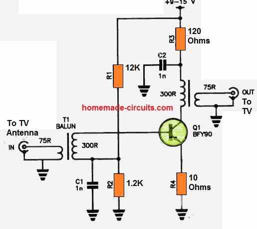
A wideband, low noise VHF amp is shown in the following figure to improve TV or scanner reception. It is easy to construct and presents no problems.
There is no optimizing needed.
The signals coming in are coupled to the base of transistor Q1, a BFY90, using a typical 75 to 300 Ohm TV antenna balun. R1-R2 produce the base bias, which is then bypassed by C1 and the 300 Ohm winding of T1.
R4 offers some emitter degeneration [negative feedback] for Q1. Similar to T1, another balun links signals to the output connection.
The output transformer's 300 Ohm winding serves as the source of the collector voltage for Q1, which is then bypassed by C2 and decoupled by R3.

Comments
Hi
On my small boat I have a handheld 1w/5w vhf. 160 to 170 odd mhz. It struggles to transmit more than a few miles. Have you a circuit for a 12v RF amplifier up to 25w.
I’ve mounted the vhf inside with a permanent 12v to 9v power supply and a speaker/mic. I’ll mount an external antenna – any advice on that.?
Hi, yes, I have an article related to RF amplifier circuits, you can find it in the following link.
https://www.homemade-circuits.com/rf-amplifier-and-converter-circuits-for-ham-radio/
Actually your VHF handheld is fine but if range is bad then mostly the antenna setup is weak. Before thinking about boosting to 25W, first try mounting a good vertical antenna like a 5/8 wave whip or marine dipole on top of your boat, as high as you can. Even 5W can go 20 km over water if antenna is high and tuned well. About the 25W booster, yes you can use a 12V RF amplifier using a final stage like MRF247 or SD1446 but that needs heatsink, tuning, and low pass filter to avoid harmonic mess. Also remember boat vibrations and water salt can mess up cheap circuits so box everything well.
Thank you for your reply. I’ll try a better antenna as suggested first.
Sure, no problems..
Hi Swagatam. I need a little help with a project. I want to build a high gain (50+db at least) RF wideband amplifier with power supply, tunable at 5Mhz-8Mhz and 0-180 degrees power shift at will.Do you have any idea?
Thanks Nikos, I wish I could help you, however designing a high frequency based amplifier looks difficult for me and I do not have the necessary formulas for it…nevertheless i will try to find it online, if I happen to find it, will surely update it for you here.
hi swag
is it possible to filter out unwanted radoi stations from from antenna .and if so how do you do it?
Hi Way, to filter out unwanted radio stations you will need an adjustable LC tank circuit after the antenna stage.
hi swag
do you know were to source bfy50 transistor or its equivalent?
Hi Way, you can simply replace it with a BC547 transistor…
hi swag
which on of your wideband amplifier circuits would you use to boost AM band antenna signal for am radio reciever. IE simplest AM radio circuit ?
Hi Way, I think you can try the first circuit, that looks most appropriate for the AM bands.
Currently living in Costa Rica, I do not have access to the components for which I wish. Some minor supplies I have.
Could You please supply the circuit for a 50 to perhaps 100 watt amplifier capable of providing a somewhat stable output at 465 kHz…but a circuit that does not use FETs.
Thank You,
A 50 watt to 100 watt 465 kHz wideband amplifier circuit using only BJTs looks difficult. I don’t have this circuit with me at the moment, but if I get it will try to update it here for you
I thank You for your efforts.
Alan
It’s my pleasure!
Hi sir, I want to amplify a voltage signal within 2.3V to 2.6V, i.e, when the input is 2.6V output should be 5V and when it is 2.3V ,output should be 0V. I’ll be taking the input voltage values from WCS1800 Hall Current Sensor. It would be really grateful if you could provide me the required circuit diagram and component values
Hi Joseph,
It can simply done using an op amp comparator, but that will require an external 5V DC supply also.
no sir…actually i want a complete set of output values and not just 5V and 0V, the values should vary between the range of (0 to 5)V. when it 2.3V output @0V, when it is 2.45V output @ 2.5V and when it is 2.6V output @5V. the complete range of input should be amplified or converted into 0 to 5V without any microcontroller sir.
Joseph, if you need a specific voltage output at a specific input, then you may have to use zener diodes in that sequence, and for accurate voltage level outputs you may need opamps, and this opamp will need an external 5V supply input.
is there any circuit diagram that can meet this requirement sir….it would be very grateful if you could provide some…i’m just a sophomore
I can design one using op amps with an external 5V DC.
Please specify the maximum current output.
it can be within 2A sir
Hi Joseph, just one more question, should the output voltage rise gradually, in a proportionate manner, or do you just want the following specific levels:
@2.3Vinput, output = 0V,
@2.45Vinput, output = 2.5V,
@2.6Vinput, output = 5V,
yes sir a gradual rise
Joseph, it looks difficult, because the input/output relation in your circuit is not linear and proportional.
An input range between 2.3V and 2.6V should produce an output voltage between 2.5V and 5V, that is not linear at all.
So, unfortunately it may not be possible using a discrete circuit.
Hello Sir , I need a circuit Amplifier Out put to the Microphone input or any device input line. I have tried to connected a amplifier speaker out line to the Mobile microphone input Port and the mobile damaged . Please help me to complete my Project Sir. Have a nice day
Hello Jobayer, You can try adding a 1uF capacitor in series with the input/output connection, this will safeguard your devices from getting damaged.
Sir Could you please check the diagram. I will be very grateful to you. Purpose of the diagram is to connect amplifier output to microphone In. Thank you
https://drive.google.com/file/d/1TTipg-WRCatht3_8RxeyovDsAh3vNPzw/view?usp=sharing
Hi Jobayer, it should work, just connect a 1k resistor between the 1uF junction and ground.
Dear Sir I have been with you since last 10 years. Please help me.
I want to connect my bluetooth audio output speaker line to one of my Sound recorder module (ISD1820) microphone. Please help me to solve this issue.
Thank you so much Jobayer, for being a dedicated reader of this site. I appreciate it very much.
However, unfortunately, I have not studied how the (ISD1820) microphone works, therefore at the moment I am unable to answer your question. If possible i will investigate the circuit and try to solve it for you soon.