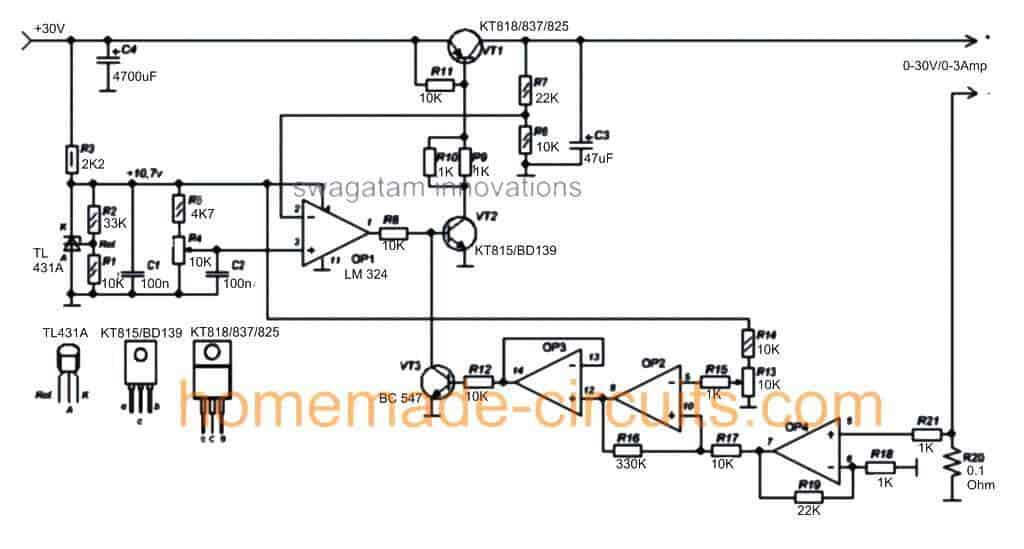
The presented universal power supply circuit can be used just for anything, you can use it as a solar battery charger, bench power supply, mains battery charger circuit, or for any desired application regardless of the voltage and current range, which are extremely flexible and fully adjustable.
Main Features:
The mains features of this power supply is that it is highly flexible, and will allow you to get a variable voltage from 0 to 30 V, and a variable current from 0 to 3 amp. Both the parameters can e controlled through a potentiometer.
The current limit can be upgraded by suitably increasing the rating of VT1, and by adjusting the value of R20.
Using a Single LM324 as the Main Control Device
The design of a simple opamp based power supply is not complex and utilizes ordinary parts such as IC LM324, a few BJTs and other associated passive components, yet it is too flexible and can be calibrated to any desired voltage and current range, right from 0 to 100V, or 0 to 100 amps.
I accidentally found this design from an online website and found it quite interesting, although I already have a similar design published in this site by the name zero drop solar charger circuit, the above shown circuit looks more meticulously designed and therefore is more accurate.
Referring to the above proposed universal power supply circuit diagram, the functional details can be understood with the help of the flowing points:
How the Circuit Functions
The IC LM324 forms the heart of the circuit and becomes responsible for all the involved complex processing.
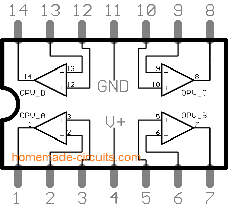
It's a quad opamp IC meaning it has four opamps in one package, and all the 4 opamps (OP1----OP4) from this IC can be seen effectively employed for their respective functionalities.
The input supply which is derived either from a mains transformer or from a solar panel is suitably stepped down using a shunt zener network VD1 to provide a safe operating voltage for the IC LM324 and also for generating a stabilized reference for OP1 non-inverting input, via R5 and preset R4.
OP1 is basically configured as a comparator, wherein its pin3 is applied with a set reference, and its pin2 is connected with a potential divider across the output of the power supply for detecting the final voltage across the load.
Depending upon the setting of the R4 which can be a pot, the OP1 compares the level of the output voltage delivered by VT1 and trims it down to the specified level. Thus, the pot R4 becomes responsible for determining the effective output voltage and can be adjusted continuously for getting the desired voltage across the indicated output terminals of the circuit.
The above operation takes care of the variable voltage feature of the proposed universal power supply circuit. VT1 and VT2 must be appropriately selected as per the input voltage range for enabling the devices to perform correctly without getting damaged.
The variable current feature of the design is implemented through the remaining three opamps, that is collectively by the opamps OP2, OP3, and OP4.
OP4 is configured as a voltage sensor and amplifier, and it monitors the voltage developed across R20.
The sensed signal is fed to the input of OP2 which compares the level with a reference level set by the pot (or preset) R13.
Depending on the setting of R13, OP2 toggles OP3 continuously such that the output from OP3 switches off the driver stage VT1/VT2 whenever the output current tends to go above the fixed level (set by R13).
Therefore R13 here can be effectively used for setting up the maximum allowable current across the output for the connected load.
The resistor R20 may be appropriately dimensioned for calibrating the maximum allowable current for the load, which can be tweaked by R13 from 0 to maximum.
The above versatile features makes this universal power supply circuit extremely efficient, accurate and fail proof so that it can be used for most electronic application one can think of.
The design can be expected to be fully short circuit and overload protected, provided VT1 and VT2 are appropriately cooled by mounting them over adequate heatsinks.


Comments
Hi all! Here is the original of this scheme https://vrtp.ru/index.php?act=categories&CODE=article&article=2349, many people repeated it. КТ818 is very old russians transistor, “datasheet” is here https://www.5v.ru/ds/trnz/kt818.htm. KT825 = TYPE147G, but Darlington’s type is not very suitable for this (the tendency to self-excite increases). It’s best to use a regular high power pnp transistor around 60..80V/10..15A, I used a 2N6491. Someone’s circuit was excited due to poor quality LM324, a capacitor with a capacity of 150-470 pF between pins 1 and 2 solves this problem.
What are your specifications for vT1? KT818/KT837/KT825? I cannot find datasheets for any of those transistors. And while I can imagine a variety of substitutes, I wondered exactly what did you have in mind with those particular devices? i.e. why those, and not others?
This is not my design, so the transistors were not specified by me.
However, the values of the transistors will depend on the output requirement by the load. Meaning it depends on the maximum voltage and current specifications of the load.
If you can provide the maximum specifications of the load, i can help you to figure out the exact transistor equivalents.
Hi Swag,
Can you place the list of components of the above circuit.
I can’t figure out what type of resistors are R7, R8, R3 and other similar.
Best Regards.
Nélio Abreu
Hi Nelio,
I am feeling too lazy to do it, but I may consider updating it sometime sooner.
The resistors which are marked with two slanting parallel lines are 1/4 watt 1% MFR,
The R3 resistor is a 2 watt 1% MFR resistor.
The R20, 0.1 ohm can be a 2 watt wire-wound type resistor.
The rest of the resistors are all 1/4 watt 5% CFR.
Hi,
What P controls voltage and current?
Best Regards.
Nélio
Hi, the 10K pot connected at the pin3 of the opamp controls the output voltage.
Thanks.
Best Regards.
Nélio
🙂 Ok.
Dear Sir, I want to make a 0-60V, 0-40A Variable power supply circuit and vary the same using a 0-5v external analog reference instead of a potentiometer. What changes should I make to the circuit above to achieve the same. Kindly advise.
Hi! While your specs are commendable, I hv 2 say that your specs are2 formidable for few reasons. It needs an equally formidable knowledge on putting together a practical Ckt with rather beefy components for one thing. And another factor is that there design that u propose can be only recommended as a bench pwr unit and not as a “drop in” replacement because it is a linear unit where the pwr dissipation would be pretty intense and inefficient. Therefore you should either dilute ur requirements or go directly to assembling an SMPS unit which will perform rather elegantly here for which many gd designs are floating around the Web. Have a nice day!
Hi Ananth,
I think you can try the following circuit, disconnect the (+) input of the op amp and connect it with your 5V supply:
https://www.homemade-circuits.com/universal-variable-power-supply-circuit/
Yes sir that works but I can only supply a max supply voltage of 30V to a LM324 opamp and hence the output of the opamp will vary from 0- 30V. How do I increase this voltage to vary from 0-60V at the final output of the circuit. Please advise.
If you are referring to the LM324 circuit published in the above article, then I think 60V is possible, because the supply pin of the LM324 is stabilized with TL431 IC
Yes but even the TL431 can only regulate voltages between 2.5 to 36V at most. Is there any other IC which I can use instead. Please advise.
I think you can search for 100 V Opamp, you would be able to find a few good options
Dear Sir, I don’t have PNP Transistors, meanwhile I found some 2N3773 from the junk dealer. So I tried to configure the circuit at : https://drive.google.com/file/d/1ZGBvVr7mWW5TMT8fi2tio5IWyQM5G8GP/view?usp=sharing Can you please examine and suggest necessary corrections ?
Thank you very much for valuable advice.
Dear Imsa, if Q1, Q2 were PNP transistors and you have replaced them with NPN transistor then that might not work. PNP cannot be replaced with NPN transistors.
I am an led manufacturer, based in Pune.
Kindly connect for PCB design/design validation and trouble-shooting work at
Thanks in advance
Sorry I don’t do freelance job.
Can you suggest a simple circuit to achieve variable power charger circuit which can be used to charge different devices from the same charger . like phone and laptop from a single charging brick.
I can use the following components if needed:
IC 7805 , Arduino
Arduino is not required, you can customize the following concept:
https://www.homemade-circuits.com/regulated-car-battery-charger-circuit-for-garage-mechanics/
Hello again, commented on the transistors in parallel. I really like this design. I assume I could use a couple 2n3055s in parallel. The supply that I am going to build will be 0-36v, 0-25a. Could you comment on any other changes to increase the current capability of this circuit.
Thanks again,
Ken
2N3055 is a NPN while the main device above is a PNP, so you may have modify the design considerably for using 2N3055s
You can try one of these designs:
Voltage Regulator Circuits using Transistor and Zener Diode
Hi Swagatam,
According to your instructions, I used both (4905,9540) MOSFET, but the output voltage did not change at first and remained high.
After that, I changed the two resistors (R9,R10) to 200 ohms and the voltage changed a little, but still irregularly and with a slow rhythm from top to bottom.
Thanks in advance for your guidance to tell me what I need to do to be able to have good control over the voltage.
Can I use the DAC on the gate of Mosfet with a feedback from output to have high accuracy in output voltage?
Hi Saed,
A P-MOSFEt should work exactly like a PNP BJT in this circuit according to me. You can connect an LED in series with the op amp output 10k resistor to make sure that the NPN does not conduct due to any leakage voltage. Plese confirm with a power BJT again, If the circuit works with a BJT then it should definitely work with a mOSFET also.
Sorry I can’t figure out how a DAC would help in this situation?
Hi Swagatam,
First i want to thank you for sharing this design I made it last night and it worked great(with Tip36 for t1 and Tip122 for t2).
The need I have for my project is about max 30v and 10 amper for continous using.
I can not use big heatsink for tip36 but I can use 12v fan instead.
I connected a 100-watt 12-volt lamp to the power to test, and within five minutes the temperature of my rectangular heatsink was extremely hot(2cm*3cm*6cm heatsink).
What can I do for reducing the temperature?
Do I have to use another transistor or can I connect the same transistor in parallel in groups of two or three or more so that the temperature rises less?
Hi Saeid, Glad you could make it successfully, yes you can put more transistors in parallel for reducing the heat, or replace the transistor with a P channel MOSFET, such as IRF4905 or IRF9540 etc
I thought we could change the voltage because of the operation of the transistors at their linear point in this power supply. And we do not have this linear state in MOSFETs.Where is my view wrong?
And if MOSFET can be an alternative, which part of the circuit should I change?
Best regards.
The circuit is not actually linear by nature, since it is not being used in the emitter follower mode. Nonetheless, a MOSFET is also a transistor and can be used in the linear mode if required, although here the VT1 is not connected to behave as a linear regulator.
You can change VT1 with a P-channel MOSFET
Dear Sir, In the circuit above, can I use HGTD8P50G1 (500V 8A) or FGA25N120ANTD (1200V 50A NPT Trench IGBT) for VT1 ? if yes, what are the other changes required in the circuit? I like to have 100~120V Output to charge 12V 40Amp batteries in series.
Thank you very much for your valuable advice.
Imsa Naga
Dear Sir, thank you very much for the express response… I’ll first try the circuit with the FGA25N120ANTD and get back to you for further advice.
Thank you once again
No problem Imsa, please go ahead!
Dear Imsa, according to me no changes will be required except the VT1, which you can replace with your own power device.
It seems R3 will also need to be changed with a 10k 5 watt resistor
Sir,
Can you please help me with a schematic for regulating DC voltage from 0 to 100V, and Current from 0 to 100 amp. Fixed Voltage Source of 100V and 100Ampere is available.
Akash, using a linear regulator for 0 to 100 V can make the transistors very hot at lower voltage adjustments, so it is not recommended,, and SMPS can be extremely complex, so i have no idea about it at this moment.
Sir,
1. Limiting the circuit to 30V regulation, can we increase the output current rating to 0-20A ?. If possible what changes may be required ?
2. The transistor KT818/837/825 all are seemed to be obsolete. Can you please recommend an alternate part number which can purchased from Digikey/Mouser.
Akash, to get 20 amp at the output, the input must be rated at above 20 amp.
You can replace the transistors with TIP36 for VT1 and TIP122 for VT2
Good day sir
May I ask what are the input signal requirements of this circuit?
redriot, you can use a 35V DC 5 amp at the input
Yes, that is correct Sir, but what i do not understand is that the sens resistor is in series with my load through the output and my output volts = 60 and output amps = 100 and that means 6000 watt. How is it possible for the sense resistor to withstand that current being rated at only 20 watt.I have mentioned to you before that i do not know how to design circuits, can only build them. Now if i look at this circuit, i see my negative output gets connected to R 21 for sensing, i think, and through sense resistor to ground.Negative output also connected to BC 847 emitter (ground),VT 2 emitter (ground), OP-AMP PIN 11 (ground), R 6 (ground), VD 1 A (ground), R 13 (ground) and C 4 negative (ground), So to me it looks like my sense resistor is in series with my output. Now Sir, please correct me if i am wrong, C 4 negative is the MAIN GROUND and that is why my sense resistor will not burn at above mentioned output levels. C 4 is a smoothing capacitor and for my output specs, what micro farad do you suggest C 4 Sir. I have read somewhere that a 1000 micro farad per amp is adequate? (i know the cap volts must be much higher than input volts, 100 to 140 volt.) Is that correct Sir and if C 4 is the main ground, that track will need to be off the PCB to be able to carry the current and of course all the other grounds must also be connected to C 4 ground ? For my output specs, what value and watts must R 3 be and what watts must all the other resistors be. Is VT 1, VT 2 and the sense resistor the only components that need to change for my output specs?
I am so sorry to bother you with all these dumb questions, but by asking dumb questions, so that i do not make stupid mistakes Sir.
Thank you very much for your patience Sir.
Hi Ian, as you can see your 100 amp value has been considered in the formula, and still we get 20 watt as the result. That means the resistor is capable of handling this current. The wire inside the resistor will be thick enough to handle this current. The 20 watt actually signifies the heat dissipation capacity of the resistor here, not the current handling capacity. At 20 watts the resistor will become hot but still will be safe enough not to melt or fuse due to the generated heat.
I hope this explanation might have solved your doubts regarding how a 20 watt current limiting resistor would handle 100 amp current in the power supply circuit.
For calculating the filter capacitor you can refer to the following article:
https://www.homemade-circuits.com/calculating-filter-capacitor-for/
Thank you Sir. And the resistor values and watts that i asked for? And other component replacements, if necessary, that i have asked for in previous question? You gave me the transistor specs via e-mail for my output levels, but surely some of the other component values need to be upgraded for my output specs?
I will run this power supply at maximum output for maximum 5 hours per day Mr Swagatam. I will use massive heat sinks and overkill cooling fans. All the power transistors and large current lines will be off the control board and i will use solid copper bus bars for those lines. If there is a small percentage of noise (ripple) in the output, it is okay for my purpose. I repair old dc welding machines and that is where i get most of my high power components from, like rectifiers, caps, cooling fans, transformers and power transistors. This power supply i want to use for anodizing aluminium parts that i fabricate for my own projects.
Thank you Mr Swagatam.
Hi Ian, all resistors are 1/4 watt 1%, except the collector resistor of VT2 which can be 1 watt 5% each. R20 will be 20 watts wirewound type.
Rest all can be as is.
I wish you all the best for the project.
Haven’t you run into stability issues with this circuit? I do not see any frequency compensation.
It is a linear power supply, not an SMPS
This circuit uses a PNP pass transistor, the configuration is similar to a low drop out linear regulator which are by nature difficult to stabilize as the poles can shift depending upon input conditions and load, there is a high chance this circuit can oscillate or give a lot of ringing on the output. This seems to be one of the reason why most commercial linear power supplies use an NPN pass transistor as that design is inherently more stable, I have been trying to tame a similar circuit lately but it so far has been hopeless really.
Thanks for pointing out the issue. Did you you try theory explained in the following post? I think if the LDO feature is removed by modifying the PNP pass transistor into a PNP/NPN Darlington might solve the issue, as explained in this article:
https://www.analog.com/en/analog-dialogue/articles/low-dropout-regulators.html
Then sorry, I do not have any solution for this impossible looking problem….you can ask in Stackexchange electronics forum.
Still getting hot.