A transistor or BJT multivibrator is a two-stage switching circuit that is configured in a cross-coupled manner. This allows each of the active BJT stages to be regeneratively cross-coupled with the other BJT stage, so that one switches ON when the other switches OFF, and vice versa.
This cross-coupling may be set up to switch either a stable or semi-stable manner. Whenever a stable cross-coupling is required, the transistor switch continues in either an ON or OFF condition until an external signal input forces it to change.
Once the circuit is cross-coupled in a semistable mode, the transistor originally latches into an ON or OFF position. However after some delay, as specified by the RC time constant of the cross-coupling, the transistor immediately gets "unlocked" again.
Types of Transistor Multivibrator
Figures 1 to figure 4 illustrate circuits for the four most basic types of transistor multivibrator circuits.
- Bistable: A bistable transistorized multivibrator can be used to generate a fixed ON or OFF output states in response to the pressing of a push button.
- Astable: In an astable multivibrator the transistors switch ON/OFF alternately and this cycle continues indefinitely as long as the circuit is powered. The switching frequency is determined by the RC components of the circuit.
- Monostable: In a transistorized monostable circuit, the output can be switched ON momentarily for a desired period of time by pressing an associated trigger button. The time delay is decided by the RC timing component of the circuit.
A triggered bistable (two stable state) multivibrator example is shown in Fig. 1, which can be triggered manually.
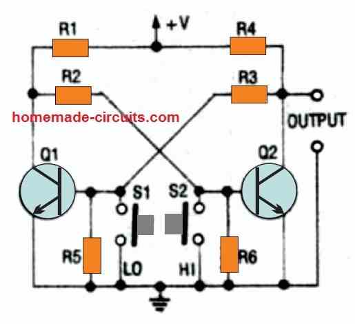
Each transistor's base-bias is derived through the collector of the second transistor, causing the first transistor to switch off when the second transistor turns on, and vice versa.
By momentarily shutting off Q1 with S1, the output may be pushed low; the circuit will remain in this condition until Q2 is switched off by S2.
The output locks into the high state at that point, and the process could be repeated for so long as the circuit remains energized.
A monostable (single stable state) multivibrator or one-shot pulse generator circuit is shown in Figure 2.
The output of this configuration is normally low, however if Q2 is momentarily switched off with S1, it turns high for a certain duration of time (defined by the values of C1 and R2).
Astable Multivibrator
An astable (without stable states) multivibrator or free-running square-wave generator is shown in Figure 2.
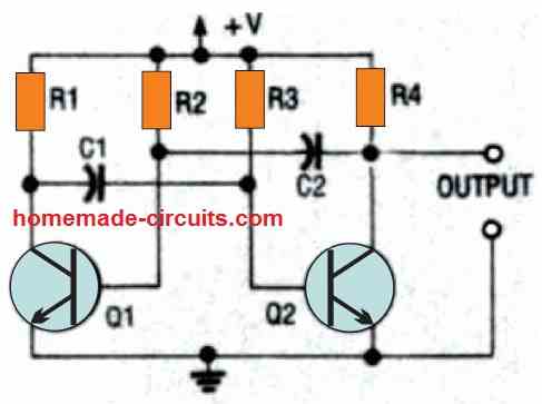
The values of R3 and C1, as well as R2 and C2, define the square wave's on and off times.
A Schmitt trigger, often known as a sine-to-square waveform converter, is shown in Figure 3.
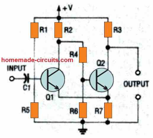
Transistor Q2 quickly flips from ON to OFF, or vice versa, when the base of transistor Q1 rises above or falls below the predefined trigger voltage thresholds.
The following paragraphs explains the above 3 basic transistor multivibrator circuits in more details:
Monostable Transistor Multivibrator
The triggered pulse generator in Fig. 4 indicates an example of a monostable multivibrator circuit.
Normally, R2 drives transistor Q2 into saturation, resulting in a low output (derived from transistor Q2's collector).
Under this circumstance, transistor Q1, which gets its base-bias via transistor Q2's collector and resistor R4, is switched off, and its collector is now at 100% supply voltage.
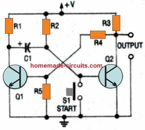
When switch S1 is briefly closed, a START signal is applied to Q2. Q2 turns off, forcing the output high and turning on Q1 via R4. The switching off of S1 causes regenerative switching activity.
When the regenerative reaction is implemented, the charge on C1 drives the base of transistor Q2 negative.
Through R2, C1 begins to discharge. Its charge finally drops to the point where Q2 switches on again, causing the triggering of yet another regenerative reaction.
Next, the output pulse stops, and both transistors restore to their original states, completing the circuit's activity.
Therefore, when an input trigger signal is applied by briefly shutting switch S1, a positive-going pulse is created at the output of the monostable multivibrator circuit. The values of R2 and C1 define the pulse period.
The following equation provides the relationship:
Pulse Period = -0.7 x R2 x C1
The pulse time is measured in microseconds, C is measured in microfarads, and R is measured in kilohms. Simply activating a momentary switch or supplying an input command signals can both trigger the circuit in Fig. 2.
A negative pulse applied to the base of Q2 or a positive pulse applied to the base of Q1 can be used as the trigger signal.
A realistic design for a mechanically triggered monostable multivibrator is shown in Figure 5-a. It may be initiated by delivering a positive pulse to Q1's base via R2 using the momentary switch S1.
The waveforms of the circuit are shown in Figure 5-b. While operating, the base-to-emitter junction of Q2 is reverse-biased by a peak voltage which is equal to the supply voltage level, as shown in Fig. 5.
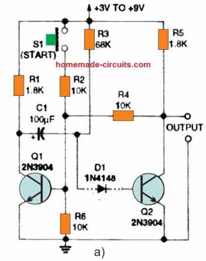
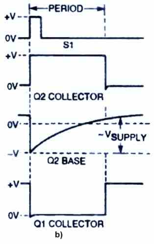
This implies that to avoid damage to the transistor, the maximum supply voltage must be restricted to around 9 volts.
If silicon diode D1 is connected in series with Q2's base, a supply voltage larger than the reverse base-emitter breakdown value of Q2 can be reliably supplied, as illustrated in Fig. 5 .
In the Fig. 5 circuit, the magnitude of timing resistor R3 has to be significantly bigger compared to R1, but lower than the product of R5 and the hFE of Q1.
The pulse time in Fig. 5 is 50 milliseconds divided by the value of capacitor C1 in microfarads. With the value of Cl as indicated in the diagram, pulse timing output will be 5 seconds.
Transistor Multivibrator with Delay Periods
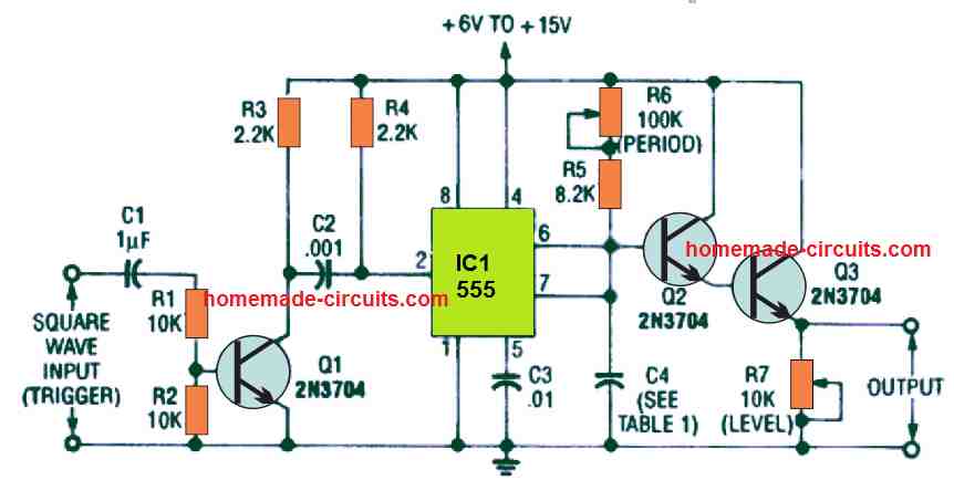
When Q2 in Fig. 5 is replaced by a Darlington transistor combination, the circuit may give very long timing intervals. As demonstrated in Fig. 6, this replacement leads to a very relatively high hFE and allows for the use of large R3 values.
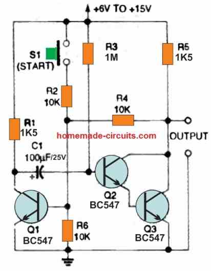
With the values of the resistors and capacitors illustrated, the Fig. 6 circuit may be supplied through any DC source with an output between +6 and +15 volts to produce a pulse output length of roughly 100 seconds.
Please remember that the length of the input trigger signal is critical for a manually triggered monostable circuit like those shown in Figures 5 and 6.
When a positive-going pulse is supplied to the base of Q1 in Fig. 5 or Q3 in Fig. 6, the circuit is activated.
The period will finish regeneratively as soon as this pulse is withdrawn before the monostable multi-vibrator ends its usual timing period, as earlier mentioned.
The timing cycle will finish non-regeneratively in case the trigger signal has not been eliminated within the period the monostable achieves its normal timing period.
The output pulse would have a longer duration and fall time as a result of this compared to if the trigger signal was terminated sooner.
How to Trigger Using Waveforms
Figures 7 and 8 demonstrate two different approaches of activating the monostable pulse generator using input waveforms. A square-wave input signal with a brief rise time triggers the circuit for each scenario.
The differentiation circuit, which consists of C1 and R1, differentiates this waveform to generate a short activation pulse.
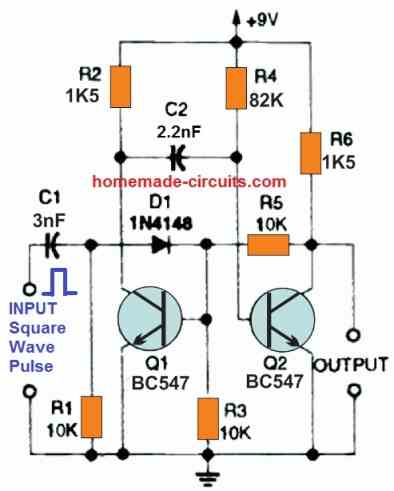
The differentiated input signal is rectified using diode D1 in the Fig. 7 circuit, resulting in a positive trigger pulse at transistor Q1 base, in case an external trigger signal is introduced.
However, the differentiated signal is supplied to the gate of transistor Q1 in the Fig. 8 circuit.
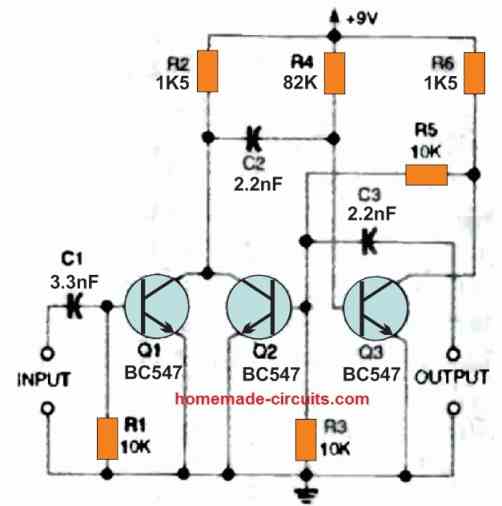
The trigger signal has now become independent of Q2 due to this alteration in the design. To optimize the structure of the output waveform, "speed-up" capacitor C3 is hooked up in parallel with feedback resistor R5 in Fig. 8.
With the indicated values of resistors and capacitors in Figs. 7 and 8, both circuits produce an output pulse duration of roughly 110 microseconds.
With appropriate values for the capacitor C2 and resistor R4, this duration may be adjusted through a fraction of a microsecond to many seconds.
When regulated by a Schmitt trigger or equivalent sinewave-to-squarewave converter circuit, the circuits in Figures 7 and 8 could be activated through a sine wave or other non-rectangular waves.
Transistor Bistable Multivibrator circuits
Figure 9 shows a realistic design for the mechanically triggered bistable multivibrator depicted in Figure 1 and explained before.
This circuit is also characterized as a R/S (reset/set) flipflop and is a rudimentary digital memory, similar to a SPDT switch.
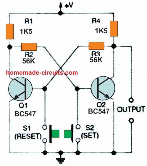
By briefly locking switch S2, the output could be set to the high state. (Put another way, apply a negative pulse to the base of Q2.)
The circuit subsequently "remembers" this condition until S1 is momentarily closed, resetting it to the low state (which can be also done by applying a negative pulse to the base of Q1).
This new state is then "remembered" by the circuit until S2 resets it. For so long as power is supplied, the cycle keep repeating forever.
A couple of guiding diodes (diodes D1 and D2) and accompanying parts could be added to the circuit in Fig. 9 to give a divide-by-two or counting function, as illustrated in Fig. 10.
When a negative-going trigger pulse is supplied to the Fig. 10 circuit, it switches state.
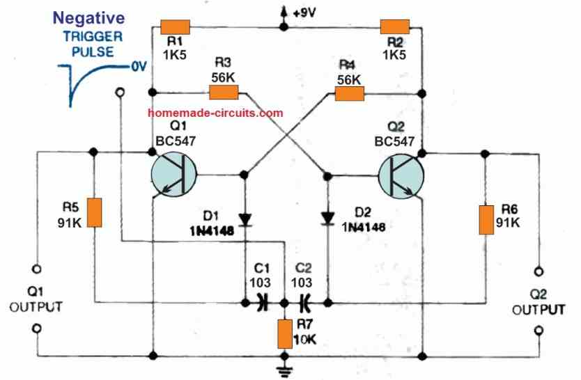
The circuit will create a squarewave output signal at 1/2 the input frequency in case for example the input pulses are generated from a squarewave pulse.
The circuit creates a couple of 180° out of phase output signals, designated Q1 and Q2. The arrival of CMOS IC equivalents of bistable counter circuits has essentially eliminated the requirement for discrete transistorized assembly of such multivibrator designs.
Transistor Multivibrators with Schmitt triggers
The Schmitt trigger circuit is the last member of the multi-vibrator family to be explored.
It's a voltage-sensitive switching circuit which switches its output state whenever the input signal rises beyond and falls below certain higher and lower threshold values.
The Schmitt trigger transforms sine waves to square waves, as seen in Figure 11.
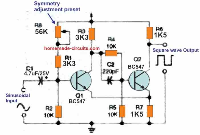
The Schmitt trigger circuit is an emitter-coupled configuration, which consists of a cross-coupling between the base and collector of transistor Q1, allowing for a regenerative switching.
By shunting R4, capacitor C2 accelerates the switching speed. A DC voltage is superimposed on the sine-wave input signal. (The voltage delivered to the base of Q1 is adjusted by trimmer potentiometer R8 and resistors R1 and R2).
A sinewave input signal having an amplitude of a minimum of 0.5 volts rms is required for an effective Schmitt trigger. R8 should be modified to maximise the uniformity of the squarewave output signal amplitude with the input signal amplitude.
At frequencies approximately to a few hundred kilohertz, the Schmitt trigger works well as a sinewave-to-squarewave converter.
The circuit can generate squarewave output signals with rise times of just a few microseconds.
Comments
Nice am gonna try one