• Skip to main content
  • Skip to primary sidebar

Homemade Circuit Projects

Need circuit help? Post them in the comments! I've answered over 50,000!

Blog | Categories | About | Hire Me | Contact | Calculators-online
You are here: Home / Electronics Theory / How to make a Transistor Latch Circuit

How to make a Transistor Latch Circuit

Last Updated on May 20, 2026 by Swagatam 179 Comments

In this post I have explained how to make a simple transistor latch circuit using just two BJTs and a few resistors.

Table of Contents
  • Introduction
    • Working Description:
    • How the Feedback from R3 Works to Latch the Circuit
  • Calculations and Formulas:
    • Threshold Voltage for BJT Activation
    • Base Current (I_B) Calculation
    • Collector-Emitter Voltage (V_CE)
    • Latch Holding Condition
    • Resistor Calculations
    • Switching Time
    • Hysteresis Voltage
    • Parts List
    • PCB Design

Introduction

A transistor latch is a circuit which latches ON with a permanent high output in response to a momentary input high signal, and continues to stay in this position as long as its in the powered condition, regardless of the input signal.

A latch circuit can be used to lock or latch the output of the circuit in response to an input signal and sustain the position even after the input signal is removed.

The output may be used to operate a load controlled through a relay, SCR, Triac or simply by the output transistor itself.

Working Description:

The simple latch circuit using transistors I have I have explained in this article can be made very cheaply using just a couple of transistors and some other passive component.

As shown in the figure transistor T1 and T2 are configured in such a manner that T2 follows T1 to either conduct and or to stop the conduction depending upon the trigger received at the input of T1.

T2 also acts as a buffer and produces better response even to very small signals.

When a small positive signal is applied at the input of T1, T1 instantly conducts and pulls the base of T2 to ground.

This initiates T2 which also starts conducting with the received negative biasing offered by the conduction of T1.

It must be noted here that T being NPN device responds to positive signals while T2 being a PNP responds to negative potential generated by the conduction of T1.

Uptill here the function looks pretty ordinary as we witness a very normal and obvious transistor functioning.

How the Feedback from R3 Works to Latch the Circuit

However the introduction of a feedback voltage through R3 makes a huge difference to the configuration and helps to generate the required feature in the circuit, that is the BJT circuit instantly latches or freezes its output with a constant positive supply.

If a relay is used here it would also operate and stay in that position even after the input trigger is completely removed.

The moment T2 follows T1, R3 connects or feeds back some voltage from the collector of T2 back to the base of T1 making it conduct virtually “for ever”.

C1 prevents the circuit from getting activated with false triggers generated from stray pick-ups, and during switch ON transients.

The situation can be restored back either by restarting power to the circuit or by grounding the base of T1 through a push button arrangement.

The circuit can be used for many important applications, especially in security systems and in alarm systems.

Calculations and Formulas:

Threshold Voltage for BJT Activation

The threshold voltage values for turning ON or OFF the NPN and PNP transistors remain the same:

  • NPN Transistor Turn-On Voltage (VBE(on)):
    VBE(on) ≈ 0.7V (for silicon BJTs)
  • PNP Transistor Turn-On Voltage (VEB(on)):
    VEB(on) ≈ 0.7V (for silicon BJTs)

These values determine when the base-emitter junction of either transistor is forward biased, enabling current flow and turning the transistor ON.

Base Current (I_B) Calculation

For both NPN and PNP transistors, the base current is still calculated in relation to the collector current:

  • Base Current for NPN Transistor (IB(NPN)):
    IB(NPN) = IC / βNPN
  • Base Current for PNP Transistor (IB(PNP)):
    IB(PNP) = IC / βPNP

Where:

  • IC is the collector current
  • β is the current gain of the transistor (typically 50–300)

This is relevant for understanding how the transistors maintain their ON or OFF states once latched.

Collector-Emitter Voltage (V_CE)

The voltage across the collector-emitter junction of each transistor is very important for ensuring the transistors remain in the active or saturation regions:

  • NPN Transistor Saturation Voltage (VCE(sat)):
    VCE(sat) ≈ 0.2V (when fully ON)
  • PNP Transistor Saturation Voltage (VEC(sat)):
    VEC(sat) ≈ 0.2V (when fully ON)

These values are relevant when the latch is "set" or "reset," which ensures that both transistors are either fully conducting or completely turned off.

Latch Holding Condition

Once the latch is set or reset, the feedback ensures that the state is maintained regardless of the input signal:

  • Feedback Current (IFB):
    IFB > IB(required)

Where, the IB(required) is the base current needed to keep the transistor latched in its ON state.

This feedback signal ensures that once the NPN or PNP transistor is turned on, the circuit remains latched in that state until forced to reset.

Resistor Calculations

Resistors will control the currents flowing through the transistor and define the behavior of the circuit:

  • Base Resistor (RB):
    RB = (Vinput - VBE(on)) / IB
  • Collector Resistor (R_C):
    RC = (VCC - VCE(sat)) / IC

Where:

  • Vinput is the voltage applied to the base of the transistor
  • VCC is the supply voltage
  • IB and IC are the base and collector currents, respectively

These resistor values help in controlling the current levels to properly switch and latch the circuit.

Switching Time

The switching time for the latch circuit or the time it takes for the latch to change states is determined by the charging and discharging of junction capacitances:

  • Rise Time (tr):
    tr ≈ (RB * Cj)
  • Fall Time (tf):
    tf ≈ (RC * Cj)

Where Cj is the junction capacitance of the transistor which determines how quickly the transistor can switch between states.

Hysteresis Voltage

Hysteresis ensures that once the circuit is latched in a particular state... it remains stable:

  • Hysteresis Voltage (Vh):
    Vh = IFB * Rfeedback

Where:

  • Rfeedback is the feedback resistor value.

This feedback voltage creates a gap between the switching thresholds which helps to prevent oscillation and ensurs stable operation.

Testing procedure can seen in the following video tutorial:

Parts List

  • R1, R2, R4 = 10K,
  • R3 = 100K,
  • T1 = BC547,
  • T2 = BC557
  • C1 = 1uF/25V
  • D1 = 1N4007,
  • Relay = As preferred.

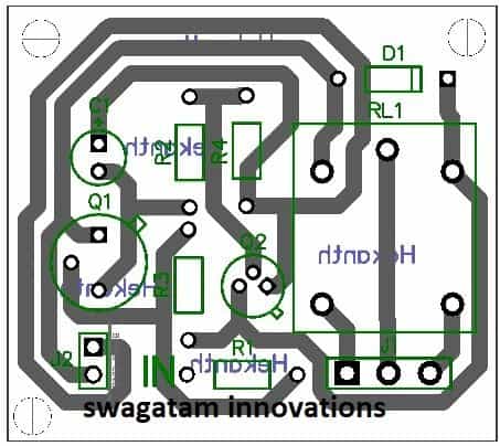
PCB Design

PCB design for transistor latch circuit

You'll also like:

  • electretHow Electret Microphones Work – Full Tutorial and Diagram
  • 1Understanding Capacitor Codes and Markings
  • triac ACTriacs – Working and Application Circuits
  • IGBT absolute maximum ratingWhat is IGBT: Working, Switching Characteristics, SOA, Gate Resistor, Formulas

Filed Under: Electronics Theory Tagged With: Latch, Transistor

About Swagatam

I am an electronics engineer and doing practical hands-on work from more than 15 years now. Building real circuits, testing them and also making PCB layouts by myself. I really love doing all these things like inventing something new, designing electronics and also helping other people like hobby guys who want to make their own cool circuits at home.

And that is the main reason why I started this website homemade-circuits.com, to share different types of circuit ideas..

If you are having any kind of doubt or question related to circuits then just write down your question in the comment box below, I am like always checking, so I guarantee I will reply you for sure!


Previous Post: « Vehicle Immobilizer Circuit Explained
Next Post: Remote Control Circuit Using FM Radio »

Reader Interactions

Questions & Answers

Total Posts: 179
Newest Oldest
justin barnes
November 28, 2025 • 9 months ago #192612

so is this circuit sort of like a scr latch?

Reply
SwagatamAdmin
November 29, 2025 • 9 months ago #192746

Yes, it is like an SCR latch.

Reply
Luciano
July 8, 2025 • 1 year ago #184254

Good morning Mr. Swagatam. As input trigger I should use a photoresistor hit by a high brightness flashing led external to the circuit. Can the circuit work? And how should I add the photoresistor? Thanks.

Reply
SwagatamAdmin
July 9, 2025 • 1 year ago #184275

Hi Luciano,
You can configure the circuit in the following manner:
latching a BJT latch circuit through LDR

Reply
luciano
July 10, 2025 • 1 year ago #184297

Thanks for the suggestion. I’ll build the circuit as soon as I have a moment and let you know.

Reply
SwagatamAdmin
July 10, 2025 • 1 year ago #184306

No problem Luciano, all the best to you.

Reply
Luciano
July 11, 2025 • 1 year ago #184377

Good morning Mr. Swagatam. I built the circuit and it works perfectly, but the relay works intermittently according to the LED flashing. However, I need the relay to remain permanently active. I need the circuit to activate a transmitter for remote control of an electric fence. Is it possible to modify it? Thanks.

Reply
SwagatamAdmin
July 12, 2025 • 1 year ago #184390

Good morning Mr. Luciano,
The circuit explained above is supposed to latch the relay ON permanently, as soon as the T1 gets a base trigger.
If the relay is not latching in your circuit, then something might be wrong. In your case the relay should latch and lock permanently with the very first flash of the LED. The 100k resistor feedback is what does the latching of the two transistors and the relay. I hope you have connected the 100k resistor correctly. You can try reducing it to 10k and test again.

Reply
Michael Fridolin
June 11, 2025 • 1 year ago #180655

hello thanks for the circuit idea. I have a question, if I want to directly drive say it 1A-2A LED strip instead of using relay what values i should use for R2 and R4 if T2 is TIP42 (overkill I thought but i have plenty of TIP42)

Reply
SwagatamAdmin
June 11, 2025 • 1 year ago #180668

You can surely remove the relay and use an LED instead with a suitable series current limiter resistor.
However, TIP142 cannot be used for T2, because T2 is PNP and TIP142 is NPN….so instead of TP142, you can replace T2 with TIP147, or maybe TIP127 with a heatsink. That’s all is needed.

Reply
Michael Fridolin
June 12, 2025 • 1 year ago #180786

thanks for your reply but i mean TIP42 power transistor not TIP142 Darlington. if I plan to use it what values for R2 and R4 resistor? sorry I have to ask because I am an IT guy and not have plentiful electronics basic although I love electronic since I was a kid

Reply
SwagatamAdmin
June 12, 2025 • 1 year ago #180800

Sorry, I misread as TIP142. Please let me know about the supply voltage, and LED supply voltage then I can calculate, or if you can simply add another PNP BJT such as BC557 or 2N2907 or BD140, with your TIP42 to upgrade it into a Darlington pair, then the the existing setup can be used without any changes in the resistor values….

Reply
Michael Fridolin
June 25, 2025 • 1 year ago #182690

ok, I will try Darlington tip142

Reply
SwagatamAdmin
June 25, 2025 • 1 year ago #182692

OK. …

Reply
Jedidiah
February 13, 2025 • 2 years ago #168409

Hello Sir. How can I ensure that the relay is energized and de-energize using positive (rising edge) clocks only?

Reply
SwagatamAdmin
February 13, 2025 • 2 years ago #168412

Hi Jedidiah, the following BJT latch circuit will trigger ON/OFF only through positive rising edge pulse.

setresetlatchcircuit

Reply
Jedidiah
February 14, 2025 • 2 years ago #168423

Is it possible to use one rising edge clock input position to ON and OFF the relay instead of having two positions (SET and RESET)? I have tried it out by shorting the SET and RESET points to achieve this but the output remains HIGH throughout after receiving the first clock. All the reset are assumed.

Reply
SwagatamAdmin
February 14, 2025 • 2 years ago #168426

Shorting the set reset will not work for the above design. If you are trying to achieve a flip flop operation then you may have to go for an IC based circuit, doing it with a BJT circuit looks quite difficult. You can refer to the following article for more info:
https://www.homemade-circuits.com/build-these-simple-flip-flop-circuits/

Reply
Jedidiah
February 14, 2025 • 2 years ago #168431

Thank you

Reply
Jedidiah
February 14, 2025 • 2 years ago #168422

Hello Sir. I have tested the circuit as drawn… but its not latching. I have tried to include part of the previous circuit whereby I placed R2 between Vcc and base of T2 and included the 1uF capacitor between Vcc and collector of T1 as it were before. It worked!

Reply
SwagatamAdmin
February 14, 2025 • 2 years ago #168425

Jedidiah, both the versions should work without any issues, no matter whether R2 is connected across base/positive of the PNP T2 or collector/positive of the NPN T1. Just make sure to connected a 0.22uF capacitor between the base/ground of both the NPN transistors (both BC547)

Reply
Jedidiah
February 13, 2025 • 2 years ago #168416

Thank you so much

Reply
Malcolm
December 27, 2024 • 2 years ago #167581

Hi. Hope you had a great Christmas.

I’ve used the latch circuit to latch after it detects the first activation ping from a burglar alarm. This works as expected. I’d hoped the output from the latch would be enough to run a 555 timer and 4017 counter that will run relays to dial a cell phone to call me, an idea from one of your other blogs, but the output is only 1.9v I s’pose all that’s left of the 12v after voltage drop. It’s not enough to run the 555.

So the latch output is now connected to a BC547 base that is acting as a switch passing 12v to the 555, 4017 and SRD-12v-SL-C relays. But I imagine the base needs resistor. The math and required understanding has got the better of me what size resistor does it need?

Seems to work alright with the 4017 driving LEDs without a resistor but I’ve had transistors cook on me before.

Reply
SwagatamAdmin
December 27, 2024 • 2 years ago #167582

Hey Thanks, hope you too are enjoying the Holidays.
You do not need a BC547 at the output for powering an external circuit. You just have to replace the shown relay coil with your external circuit.
For adequate current you may have to replace the BC557 with a 2N2907 or an 8550 transistor.
So, the collector of this transistor now connects with the positive supply line of your 4017/555 circuit, and the negative to the common ground of the supply.

Reply
Marko
August 4, 2024 • 2 years ago #157070

I’m learning electronics in my spare time. I already know some basics about electronics and still learning. I’m trying to make an alarm that uses 4011 NAND gates for checking if the an alarm wire is broken and then it should use a latch circuit to turn on a microcontroller that turns on the speaker, leds etc.

Then after a specific time the microcontroller should turn off the latch circuit, to preseve energy. This is because I want to make a small battery powered multipurpose alarm system that could be used in bikes to prevent thefts (with vibration activated sensor/switch) or as a door alarm (with NC switch) in my apartment.

I already understand quite well how NPN and PNP transistors works, but I don’t currently understand the purpose of the C1 capacitor how it works here in the circuit.

Reply
SwagatamAdmin
August 4, 2024 • 2 years ago #157075

Thank you for your question, I appreciate your interest in electronics.
Could you please tell me where is this C1 capacitor situated?
Is it connected in series with a resistor or after the resistor and across ground?
If you can refer me to the schematic or provide the exact configuration details of the capacitor in the circuit, I can certainly help you to understand how the capacitor may work to fulfil its specific job.

Reply
Marko
August 6, 2024 • 2 years ago #157260

Actually I mean the C1 capacitor in this example latching circuit you have made. To fully undertand this latching circuit, is this a decoupling capacitor or what exactly is it called in this setup? Or is this used for some kind of filtering or debouncing prevention?

But about the alarm circuit I’m trying to make, part that would activate the latch circuit would look something like this. I have 4011 ICs for this purpose, so one NAND gate would be used for checking if the circuit is closed and another NAND gate would be used to invert the output, so it could be used by a latch circuit.

I have not yet fully planned this, but my initial idea was to keep the alarm latched for a specific amount of time and it could probably be done using your latch circuit. In this example image I posted, the 1K resistor is just there because I quickly added something to demostrate.

Why I want to keep the alarm latched is that if someone would close the circuit again, the alarm so still be on and not turn off.

alarm nand

Reply
SwagatamAdmin
August 6, 2024 • 2 years ago #157273

Ok, understood!
The C1 in the above latch circuit is used for filtering external noise and to prevent false activation of the latch circuit.
However, the best position of C1 is across the base/emitter of T1, so that the noise is filtered right at the beginning of the circuit.
If you want to latch your alarm circuit for some specific amount of time, then I would recommend you using a 555 monostable circuit.
Alternatively, you can simply use your NAND gates to create a simple monostable for the same purpose.
Let me know if you have any further doubts or questions.

Reply
Jan
March 19, 2024 • 2 years ago #150513

I want the latch to stay even if the input signal drops to 0. In my preferred solution the only way to break the latch is by switching off power. How do I achieve this?

Reply
SwagatamAdmin
March 20, 2024 • 2 years ago #150533

The circuit will stay latched even if the input signal is removed. The circuit needs only a momentary input signal to get latched.

Reply
Jan
March 20, 2024 • 2 years ago #150545

thanks for your quick reply. at the moment, the latch drops when the base resistor of T1 is connected to ground. I don’t want this to happen. instead I want the latch to stay until the power is turned off even if the input signal drops to 0. Can you suggest a modification?

Reply
SwagatamAdmin
March 20, 2024 • 2 years ago #150553

For that, you can add a 1N4148 diode at the input side of R1, and feed the trigger signal through this diode.

Reply
Jan
March 22, 2024 • 2 years ago #150639

it worked, thanks for your help
Jan

Reply
SwagatamAdmin
March 22, 2024 • 2 years ago #150643

Glad it worked…

Reply
JimmyCrackedCorn
February 24, 2024 • 2 years ago #149419

I have a circuit that takes less than 100usec to “get started” and my input signal is high during this startup period. How can I ignore the first 100usec of input before using the input to trigger? Within ~ 40usec my input is low and later (tens of seconds) the input goes high as expected and this is the transition I wish to react.

Reply
SwagatamAdmin
February 24, 2024 • 2 years ago #149422

Controlling a microsecond signal looks difficult, I can’t figure out a configuration that would control the microsecond timings with such accuracy.

Reply
Ryan
February 17, 2024 • 2 years ago #149242

Amazing! Thank you so much!.
I simulated it and it works. Just the 2 questions I have are:
1) I have a 20us negative pulse that I need this transistor to switch on to and turn on the LED. Will this work?
2) There could be a lot of noise in the signal that will trigger the base of T2. I know you mentioned that C1 should help with the filtering, but now that i have switched the input to the base of T2 would this capaitor still help with noise or should I make modifications?

Reply
SwagatamAdmin
February 17, 2024 • 2 years ago #149243

Thanks, Glad it helped.
C1 might help to eliminate false switch ON only if it is connected directly across base/emitter of T2. However if this done, then the 20us pulse will be too short and might get quickly absorbed by the capacitor, so that no signal reaches the T2 base.
Nevertheless, you can try smaller capacitor values such as 0.01uF across base/emitter of T2 and see if that helps to mitigate the noise and yet allows the 20us triggering.

Reply
Ryan
February 17, 2024 • 2 years ago #149240

I would like to know how to switch the circuit on a negative going pulse rather than positive. What changes do I need to make ?

Reply
SwagatamAdmin
February 17, 2024 • 2 years ago #149241

Apply the negative pulse to the base of T2 via a resistor.
R1 can be removed, it is not required now.

Reply
Girish Chauhan
March 6, 2023 • 3 years ago #140781

I am giving triggering of 1 volt from ccd camera video signal ,how can we make it possible to disable the latching when the trigger voltage is deactivated

Reply
SwagatamAdmin
March 6, 2023 • 3 years ago #140787

It means you don’t want the latching feature, for that you simply have to remove the R3 resistor link.

Reply
Girish Chauhan
March 6, 2023 • 3 years ago #140796

Thanks Sir

Reply
Girish Chauhan
March 6, 2023 • 3 years ago #140780

Thanks for the circuit, i made and it works fine, is there any way the the the latching will reset when the trigger circuit is removed if so please share diagram

Reply
SwagatamAdmin
March 6, 2023 • 3 years ago #140786

Thank you for the update! Triggering is supposed to be done only once, then the circuit latches and remains latched. If the circuit resets on removing the triggering source then it won’t be a latch circuit.

Reply
Cn sampath kumar
January 10, 2023 • 4 years ago #138762

In connection with previous ckt my inputs both are +ve for dis i need ckt sir.

Reply
SwagatamAdmin
January 10, 2023 • 4 years ago #138766

Try this circuit then:

set reset latch circuit

Reply
Cn sampath kumar
January 9, 2023 • 4 years ago #138719

Pl give me SR Transistor lactch ctk with detail

Reply
SwagatamAdmin
January 9, 2023 • 4 years ago #138720

here it is:

motor set reset control

Reply
Jack
August 12, 2022 • 4 years ago #132251

Built circuit but it latches on application of power. I have checked and rechecked the circuit and soldering but I am at a loss

Reply
SwagatamAdmin
August 12, 2022 • 4 years ago #132263

Connect the C1 across base/emitter of T1. C1 can be a 1uF/25V. This will stop the self latching issue.

Reply
Rahul Bansal
January 30, 2022 • 5 years ago #111044

Hi

Thank you for the post. I tried replicating the circuit with BD139 and BD140 transistors. All seems to work well, except that there is a voltage drop across T2. The input voltage is 9V, the output is only 4.5V. Why would this be heppening?

Reply
SwagatamAdmin
January 31, 2022 • 5 years ago #111092

Hi, that should not happen. The collector of the PNP must show the same voltage as its emitter supply. Did you check the voltage without a load or the relay? Please check it without a load.

Reply
Doug
November 18, 2021 • 5 years ago #104985

Hi Swagatam,
I have what I suspect is an impossible circuit, but want to run it pass you to confirm.
I am sure you have knowledge of a simple moisture tester. This device uses dissimilar metals generally made up of copper and zinc. These metals when exposed to moisture (water) give a very low electrical current, this is the basis of my question.
I would like to know if there is any circuit and or device that could be powered by say a 3.7vdc lithium Ion battery or a 1.5VDC AAA battery that is basically in the off position, until two leads senses moisture, thereby powering up and indicating by a low volt LED that there is moisture across these 2 “LEADS” dissimilar metals but wouldn’t cause any, “shock” if applied to sensitive skin?

Reply
SwagatamAdmin
November 18, 2021 • 5 years ago #105006

Hi Doug,

It is definitely possible, I have designed the circuit and have posted it at the end of the following article, you can check it out:

https://www.homemade-circuits.com/soil-moisture-tester-circuit/

Reply
KRISHEN GOPAL KATHEL
August 13, 2021 • 5 years ago #94237

For very less sensitive , what can we do as for water level sensing by 12 volt relay.

Reply
SwagatamAdmin
August 13, 2021 • 5 years ago #94275

Could not understand what is less sensitive, please explain properly!

Reply
Suresh
May 16, 2021 • 5 years ago #89586

Can latch be ‘broken’ by an input based transistor switch inserted in the connection with 110 k reactance?
If the answer is ‘yes’, can one use more than one input as ‘breakers’ ?

Reply
SwagatamAdmin
May 16, 2021 • 5 years ago #89589

yes that’s possible, as given in the following figure:

set reset circuit

Reply
Yogesh
April 18, 2021 • 5 years ago #88572

Sir, I want to create a simple latching circuit,
which can turn on/off by using single push button only.
Sir,Please note that,i want to achieve this task without using IC and microcontroller.
Please help me to design this circuit
I eagerly waiting for yours response sir

Reply
SwagatamAdmin
April 18, 2021 • 5 years ago #88575

Hi Yogesh,
You can refer to the second last circuit from the following article:

https://www.homemade-circuits.com/build-these-simple-flip-flop-circuits/

However, without using an IC, and using only transistors may not give reliable results….using IC will give extremely reliable results.

Reply
Yogesh
April 18, 2021 • 5 years ago #88576

Thank you sir,☺️????

Reply
Yogesh
April 18, 2021 • 5 years ago #88562

Sir, what is the use of resistor R4 in this circuit?
And what happens,if I won’t use R4 resistor present in this circuit?
Please clear my doubt sir

Reply
SwagatamAdmin
April 18, 2021 • 5 years ago #88567

Yogesh, R4 keeps the T2 base to a proper switched OFF condition when T1 is not conducting, which ensures that the T2 base is always held at a well defined potential and never in the floating position.

Reply
Marko
August 11, 2024 • 2 years ago #157716

The R4 is called a pull-up resistor in this case. Just in case if someone else tries to figure out how the circuit works.

But about the R3 resistor, is it really needed, or could the feedback loop use only the R1 resistor? I have some difficulties understanding the function of the R3 resistor.

Reply
SwagatamAdmin
August 11, 2024 • 2 years ago #157743

R4 is actually a pull-down resistor in this case, because T2 is a PNP transistor.
R3 is the heart of the latch circuit, without it the latching would never happen.
With a momentary base trigger when T1 is turned ON, T2 also is also turned On, which allows a feedback voltage to pass through R3 and reach the T1 base, so that now T1 and T2 lock on with each other ensuring that the circuit gets latched regardless of whether T1 base is getting any external trigger or not.

Reply
Yogesh
April 18, 2021 • 5 years ago #88570

Thank you sir, ???? now I understood
And again thanks for yours speedy response sir……

Reply
SwagatamAdmin
April 18, 2021 • 5 years ago #88574

You are welcome Yogesh!

Reply
Paul_John
April 8, 2021 • 5 years ago #88331

Hi, I simulated your circuit with 12V input but it doesn’t work as intended – can you please provide design guidelines for selection of resistors?

Reply
SwagatamAdmin
April 8, 2021 • 5 years ago #88333

Hi, the circuit is fully tested, so you can be sure it will work if you build it practically.

Reply
Paul_John
April 8, 2021 • 5 years ago #88335

I did build the circuit – is it mandatory to use BC547 and BC557? I’m trying to use BC807 and BC817 instead…

Reply
SwagatamAdmin
April 9, 2021 • 5 years ago #88340

Any NPN/PNP combination should work. It is advisable to remove the capacitor C1 from the existing position and place it across the base/emitter of T1 for better response

Reply
Dang Dinh Ngoc
March 29, 2021 • 5 years ago #88076

Hi Swag,
It me again to bother you. Can I ask you a small question. I made a copy the latch circuitry as shown on the image below (this also a copy of your schematic).
latch flip flop using transistor
+ The switch will turn on the LED1 at first press (Discharged C1 via Switch and Base of T1);
+ At the 2nd press LED1 will be off as voltage drop at Q1 then Q1 closed and turn off the LED.
In this two stages the current will run from different directions on the Switch.
Due to the nature of my project that require the load can be overridden by a touch button (in case of microcontroller failure). I need a way to control the latch using both Manual button and one I/O pin of microcontroller and can also handle state of the load (on or off) on that only one pin.
I am thinking of replacing the switch with something that allows the current from both direction (2 transistors or a triac). This will allow me to run this circuitry from a capacitive touch button or a PULL_UP pin from microcontroller. This is critical as I can
+ Turn off manually the load by using a touch button (TTP223 module) – without the use of Microcontroller and;
+ Turn off the load by using Microcontroller and can also monitor state of the load (on/off) using just single I/O pin.
Can you advice me on what part I can use to mimic the Momentary Switch button with thanks
Dang Dinh Ngoc
Vietnam

Reply
SwagatamAdmin
March 30, 2021 • 5 years ago #88099

Hi Dang, you can try replacing the push button with a bidirectional switch as discussed in the following article:

https://www.homemade-circuits.com/bidirectional-switch/

Reply
Donna
February 4, 2021 • 6 years ago #86696

Interesting circuit, thanks for sharing this. I was building one just like it for an evening class I’m following and without any capacitor I have no sensitivity issues, that’s nice I suppose. I do have a question though. It may be a stupid question, but isn’t your snubber/flyback diode forcing any current from the relay through T2 and damaging it??

Reply
SwagatamAdmin
February 4, 2021 • 6 years ago #86697

Thanks, and glad you found the post interesting.

The sensitivity issue will not be there without the capacitor if the supply is from a battery.

If you are using an AC to dC adapter then removing the capacitor will simply latch the circuit each time power is switched ON.

The back EMF is developed across the relay coil in the reverse direction such that the diode orientation allows a forward path for this EMF to get short circuited through its terminals….so it is fine, no problem with the diode orientation.

Reply
Donna
February 6, 2021 • 6 years ago #86761

Thanks for the speedy reply, very helpful

Reply
Paul
October 26, 2020 • 6 years ago #83949

Hello Swagatam,
Thanks for the circuit and description which I enjoyed making.
Just like Abu-Hafss I found it to be very sensitive to finger touch and power ups.
So I increased C1 as you first suggest and eventually moved it to between T1 base and collector which worked great. Please would explain how C1 works in preventing these problems? as I want to understand why and not just assemble things without the knowledge of their workings.

Reply
SwagatamAdmin
October 26, 2020 • 6 years ago #83952

Hello Paul, that is correct, shifting C1 across the base/emitter of the NPN is more effective for controlling the switch ON triggering of the circuit.
When power is switched ON, a voltage spike across the power line is normally developed which can cause small voltage to get through the base/emitter of the NPN and trigger it ON. The capacitor acts like a momentary short circuit which grounds this small voltage spike, preventing it from reaching the base of the NPN.

Reply
Paul
October 26, 2020 • 6 years ago #83954

Thanks Swagatam – now I understand.

Reply
Nuno Martins
June 20, 2020 • 6 years ago #79680

Hi, I’m not sure if my link went trough, I don’t see my comment. But here it is:
https://studentuml-my.sharepoint.com/:u:/g/personal/nuno_ekoyedesenamartins_student_uml_edu/EdukUKJEoQ5Phr5k8zYqvHMBzGlW6BGYIzEtVFY-pf5iLg?e=gMbATj

C1 and C2 corresponds to your circuit diagram above. Thank you!

Reply
SwagatamAdmin
June 21, 2020 • 6 years ago #79689

Hi, Please show it in a schematic format, so that I can see where the transistor base, collector emitters are going, a rough block diagram will not help.
Or you can tell me what exactly are you trying to achieve in your application, I’ll try to design it for you..

Reply
Nuno Martins
June 20, 2020 • 6 years ago #79665

It doesn’t allow me to post a picture here. But to make it simple, imagine 2 coils in series, and where these 2 coils connect is considered the positive side. Lets call the positive side A3 and the negative ends A2 and A1. I connected your diagram to one side of this coil connection. From A3 to A2 (set). This will be triggered by a 3.3v pulse and stay open until power is disconnected.
Now, I want to use the other coil to disconnect this circuit. When I send a pulse to A3 and A1 (reset) the relay will go back to Close state. Currently, i have connected your circuit to the one coil and it works as intended. I also did another same circuit connected to the other coil. I observed that Only one side works properly at a time, but not at the same time. For example if I have one side connected, and I pulse the other side to disconnect it doesn’t work. I guess it’s because it’s triggered already and it needs to be disconnected from power? What changes can I make to the reset side (second coil) so that when I pulse a signal the relay will go to Close state? I hope this is more clear, thank you!

Reply
SwagatamAdmin
June 20, 2020 • 6 years ago #79667

Please upload your schematic to any free image hosting site, and provide the link here, if it is possible I will try to solve it for you.

Reply
Nuno Martins
June 20, 2020 • 6 years ago #79651

Hello there, I’m new to electronics and I’m trying to connect this circuit to a bistable latching relay(2 coils relayRT314F05). The relay has 3 control pins (A3+ to A2- is to set/ and A1- to A3+ is to reset). So when i Connect one coil to the latch circuit works it fine. But when I add the same latch circuit on the other side to reset the circuit it doesn’t work. I found that when I trigger 1 gpio, both sides of the circuit are active therefore it doesn’t work… how can I set/reset using 2 different gpio pins without one circuit interfering the other? Operating 1 at the time. Thank you!

Reply
SwagatamAdmin
June 20, 2020 • 6 years ago #79663

Hello, without seeing the diagram it can be difficult for me to understand the fault. However, in order to reset the above latch circuit or break the latch, you will need to add another transistor circuit which can ground the T1 base.

Reply
Sam
May 3, 2019 • 7 years ago #66804

Please swagtam can i use this circuit in a 433mhz receiver circuit which has output of about 2V from ht12d output (pin 10,11,12,13).

Reply
SwagatamAdmin
May 3, 2019 • 7 years ago #66806

Hi Sam, yes you can, the circuit requires hardly 0.3V to activate

Reply
Antreas
March 13, 2018 • 8 years ago #59063

I just want to ask I made the circuit but instead of the relay, i connected an LED to light when it will latch. The problem that I have is the input is 0V which mean the LED is off because of the latch is not working but mine when the input is 0V then the LED is working and to the base of the transistor of BC547 I have 0.7V which I don’t get it.
I will appreciate if you answer me to this question.

Reply
SwagatamAdmin
March 14, 2018 • 8 years ago #59066

did you connect C1? Alternatively connect another capacitor (10uF/25V) across base emitter of T1

Reply
abba
November 7, 2017 • 9 years ago #55657

thanks a lot I now understand, its the reverse bias process from the pnp that confused me. now I got the concept. thanks again ones more. truth be told I followed a lot many website but this one is different and unique. one of the factors that made it unique is the quick response to your questions asked. I want to use this medium to say, a big thank you on behalf of all of your entire followers. thanks ones more.

Reply
SwagatamAdmin
November 8, 2017 • 9 years ago #55667

thanks abba, glad you are finding my site useful…please keep posting your thoughts, and keep up the good work!!

Reply
abba
November 7, 2017 • 9 years ago #55652

hi Swagatam, my question is, in the theoretical concept if pnp base is connected to collector of the npn transistor the circuit to me wouldn’t work because to me the base of the pnp should be grounded and the npn base should be connected to the postitve of the power supply as well as ts collector. am confuse pls explain how the biasing will take place when pnp and npn are connected in the above manner.

Reply
SwagatamAdmin
November 7, 2017 • 9 years ago #55653

Hi Abba, the exact reply to your question is already provided in the article, please read the “circuit Description” section and let me know whether you could grasp it or not, or which portion you couldn’t understand.

Reply
SwagatamAdmin
July 18, 2017 • 9 years ago #51809

Hi, did you connect C1? C1 is specifically introduced to prevent this issue.

alternatively you can shift C1 across the base/emitter of the BC547, and check the response, the issue will be completely gone.

preferably use a 1uF for C1 or above

Reply
Unknown
January 16, 2017 • 10 years ago #48115

Hello, thanks you for the post. I do have a question however. I want to activate a relay with an arduino signal (less than 3 volts). The realy needs a power supply of 9V. So When I made the connections the signal from the arduino would not trigger the latch. I tried to use a positively charged wire coming form the +9V side to activate the latch and it worked. I realized that the arduino and the battery dont have common ground so the arduino signal doesnt really mean anything to the transistor. I thought of connecting the ground of the +9V and the arduino to have common reference but then I started thinking? WHat if the ground levels of the arduino and the battery are not in the same state(which probaly they are not) That means that either the battery ground will increase in voltage therefore reducing the batteries volatage difference and then the battery will not be able to activate the relay..OR worse the battery negative will be higher than the arduino so current wills tart flowing backwards in the arduino board…and now I am compeltelly confused..how do you go around that? how does commono ground works in cases where you have different intependet power circuit conected in parallel..??

Reply
SwagatamAdmin
January 17, 2017 • 10 years ago #48133

hello thanks!

as you said it yourself, the common line is referred to as "ground" which is not "negative" rather it's a zero volt line (0V), therefore any voltage reaching this line would ultimately become "zero" therefore it is completely safe and also mandatory to connect the two grounds together so that the two units can correspond and work together.

Reply
View Older Comments

Need Help? Please Leave a Comment! We value your input—Kindly keep it relevant to the above topic! Cancel reply

Your email address will not be published. Required fields are marked *

Primary Sidebar


Categories

  • Arduino Projects (95)
  • Audio and Amplifier Projects (134)
  • Automation Projects (18)
  • Automobile Electronics (104)
  • Battery Charger Circuits (90)
  • Datasheets and Components (109)
  • Electronics Theory (150)
  • Energy from Magnets and Earth (41)
  • Games and Sports Projects (11)
  • Grid and 3-Phase (20)
  • Health related Projects (27)
  • Home Electrical Circuits (13)
  • Indicator Circuits (16)
  • Inverter Circuits (100)
  • Lamps and Lights (163)
  • Meters and Testers (72)
  • Mini Projects (28)
  • Motor Controller (68)
  • Oscillator Circuits (30)
  • Pets and Pests (15)
  • Power Supply Circuits (91)
  • Remote Control Circuits (50)
  • Security and Alarm (65)
  • Sensors and Detectors (107)
  • SMPS and Converters (46)
  • Solar Controller Circuits (62)
  • Temperature Controllers (44)
  • Timer and Delay Relay (50)
  • Voltage Control and Protection (44)
  • Water Controller (37)
  • Wireless Circuits (31)


Circuit Simulator

circuit simulator image


Subscribe to get New Circuits in your Email


Other Links

  • Privacy Policy
  • Cookie Policy
  • Disclaimer
  • Copyright
  • Videos
  • Sitemap

People also Search

555 Circuits | 741 Circuits | LM324 Circuits | LM338 Circuits | 4017 Circuits | Ultrasonic Projects | SMPS Projects | Christmas Projects | MOSFETs | Radio Circuits | Laser Circuits | PIR Projects |


Recent Comments

  • Swagatam on Simple Delay Timer Circuits Explained
  • Swagatam on SG3525 Full Bridge Inverter Circuit
  • Swagatam on How to Replace a Transistor (BJT) with a MOSFET
  • Swagatam on Inverter Circuit with Feedback Control
  • Ngwabe David on SG3525 Full Bridge Inverter Circuit

Social Profiles

  • Twitter
  • YouTube
  • Instagram
  • Pinterest
  • My Facebook-Page
  • Stack Exchange
  • Linkedin

© 2026 · Swagatam Innovations