In this post I have explained an over voltage cut-off protection circuit in the form of automotive dump load for protecting sensitive and sophisticated modern automotive electronics from transient DC electrical spikes emanating in vehicle electrical.
Transient bus voltages are a significant risk factor to integrated circuits. The maximum breakdown voltage that an integrated circuit may be specified to tolerate is determined by its style and design approach that can be predominantly low for tiny CMOS devices.
What's Transient Voltage
Transient or repetitive over voltage circumstances that defeat an IC‘s absolute highest voltage spec may possibly irreversibly harm a device.
The necessity for over voltage safety is notably prevalent in automobile 12V and 24V designs in which peak "load dump" transients is usually as very high as GOV. Certain load safeguarding strategies shunt input transient to ground through devices similar to avalanche diodes and MOVs.
The difficulty with the shunt method is that a great deal of power could possibly end up being processed.
Shunt techniques are usually undesirable should there be an obligation to render continual protection throughout an over voltage situation (as transpires with dual battery).
The Design
The Over Voltage Protection Circuit for Automotive Load Dump shown in Figure 1 is a perfect series disconnect or series cut-of circuit which has been built to safeguard a switching regulator load that possessed an optimum input voltage of 24V.
The circuit is intended from economical discrete devices and makes use of a single Texas Instruments LMV431AIMF.
Given that this circuit employs a PFET pass device (Q1), there may be a marginal forward voltage drop or related power loss.
Circuit Diagram
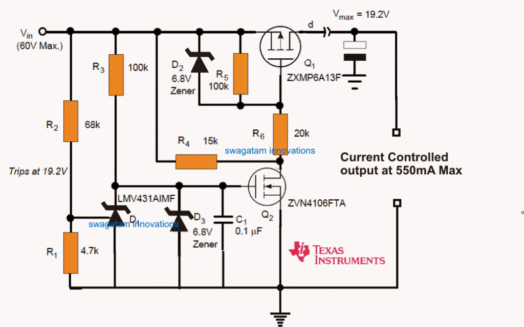
Figure.1
Courtesy: Over Voltage Protection Circuit for Automotive Load Dump
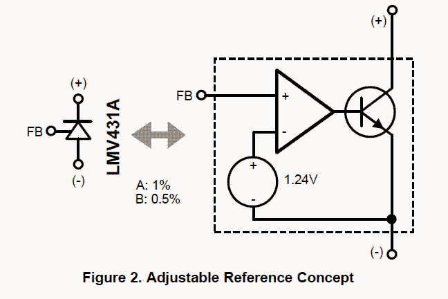
How LM431AIMF Diode Works
The LMV431AIMF (D1) adaptable reference works best for this situation just because it allows for an inexpensive means to ascertain a meticulous trip point and monitor optimal temperature accuracy which becomes quite difficult with a zener diode or likewise using other alternative options (1% for the A version, 0.5% for the B version).
For preserving this accuracy and reliability, resistors R1 and R2 is selected to be 1% tolerance or a still better may be recommended.
Variable reference voltages can be usually wrongly contemplated. Take for instance: "What’s that third wire terminating from that diode'?"
You may find numerous types of variable voltage references. Different possessing different in-built set voltage while others with an alternate current direction polarity.
All of them can be identified with a couple of fundamental (and quite significant) stages: A temperature regulated, accurate band gap voltage reference, along with a gain error amplifier (incorporated as as a comparator in the discussed circuit).
Majority of the parts exhibit uni-poIar results by incorporating an open collector or emitter. Figure 2 indicates conceptually what may be expected inside Texas Instruments LMV431AIMF.
Calculating the Cut-of Threshold
The input voltage is checked and controlled by the LMV431 with the aid of voltage divider R1 and R2. The circuit detailed in Figure 1 is configured to activate at 19.2V although an arbitrary cut of level could be opted which may be figured out using the following equations:
Vtrip = 1.24 x (R1 + R2 / R1)
R2 = R1(Vtrip/1.24 - 1)
How it Works
The output of the LMV431 brings down as soon as the set reference pin is detected to be above 1.24V. The cathode of an LMV431 is capable to bring down to a saturation level of approximately 1.2V.
The mentioned level may be just enough to switch Q2 off. Q2 was predominantly hand picked to carry an elevated gate threshold (> 1.3V). It's not recommended to use a substitution for Q2 without considering this into account.
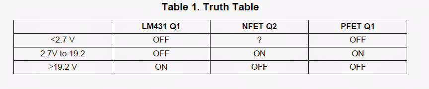
The chip operating conditions for D1, Q2, and Q1 are indicated in Table 1 for the condition involving of a 19.2V cut of point.
The circuits operating condition is detailed in Figure 3. The cut of level can be expected to be approximately in the 2.7V to GOV vicinity. Below about 2.7V the circuit may be seen transiting to the off situation.
The reason being the absence of sufficient input voltage to level up the gate to source thresholds of Q1 and Q2.
While it's in the off state, the circuit offers around 42 kQ to the input (off status quiescent load). Zener diodes D2 and D3 are crucial for restricting the over shooting gate to source voltages as expressed by Q, and Q2 (which may not be allowed to go beyond 20V).
D3 likewise inhibits the cathode of D, from shooting above its specified limit of of 35V. Resistor Rd assures a compromised bias to Q2 so that it can fulfill Q2’s drain leakage in the off condition.
It's important to watch the body diode in Q, it implies that it carries no safeguarding to the load for wrongly connected battery (opposite polarity input voltages).
To be able to safeguard the condition of a wrong battery polarity, it may be advisable to incorporate a blocking diode or an reinforced alternate (one behind the other) PFET is may be also required.
The circuit can be seen attributed to actuate instantly although reestablish the conditions rather sluggishly. Capacitor C, exhibits quick discharging to negative via the LMV431 in an even of an over voltage is sensing.
As soon as the situation restores to normal, reconnection is slightly held up by the R3-C1 time delay variables.
A significant number of loads (that may be regulators) employ substantial input capacitors which allow time delay for the cut-off circuit to work out by inhibiting the transient slew rate.
The working pattern of the standard transient and the available capacitance become responsible fix the intended delay response time.
The shut off implementation from the proposed Over Voltage Protection Circuit for Automotive Load Dump takes place in approximately twelve Sec. The expected highest transient rise periods are constrained in a balanced level to the mentioned periods by C(load).
This circuit was verified with a C(load) of 1 pF. Larger load is may be tried and is okay considering rapid surging, reduced source impedance transients are to be present.


Comments (5)
Hello!
Awsame explanation, thanks for sharing!
When the circuit enter in protection (LM431 ON -> NFET OFF -> PFET OFF), where does all the power go? What components dissipate it?
Why is it written that yours output is controlled at a maximum current of 550mA? I couldn’t see where this control is happening, can you please explain it to me?
Hi, thanks, and glad you liked the article.
In the protection mode, Q1, Q2 are turned OFF, so none of the devices are ON so dissipation becomes zero.
I cannot see 550mA written anywhere?
What would it take to make this overload protection for an older 12v motorcycle electrical system, where the regulator/rectifiers are known to degrade and fry CDIs and batteries?
One step further, could it be modified for lithium motorcycle battery?
You can use the above circuit with any motorcycle which includes an alternator for charging a battery. Yes li-ion battery can be also used in this design without any modifications, since the current is quite less and the voltage can be regulated as desired.
Thanks for the great info!