In this post I have explained how to build 10 simple yet useful function generator circuits using IC 4049, IC 8038, IC 741, IC 7400, transistors, UJTs etc. for generating accurate square waves, triangle waves, and sinewaves through easy switch operations.

1) Using IC 4049
Using only one low-cost CMOS IC 4049 and a handful of separate modules, it is easy to create a robust function generator that will provide a range of three waveforms around and beyond the audio spectrum.
The purpose of the article was to create a basic, cost-effective, open source frequency generator that is easy to construct and used by all hobbyists and lab professionals.
This goal has undoubtedly been accomplished, as the circuit provides a variety of sine, square and triangle waveforms and a frequency spectrum from roughly 12 Hz to 70 KHz employs just single CMOS hex inverter IC and a few separate elements.
No doubt, the architecture may not deliver the efficiency of more advanced circuits, especially in terms of waveform consistency at increased frequencies, but it is nevertheless an incredibly handy instrument for audio analysis.
For a Bluetooth Version you Can Read this Article
Block Diagram
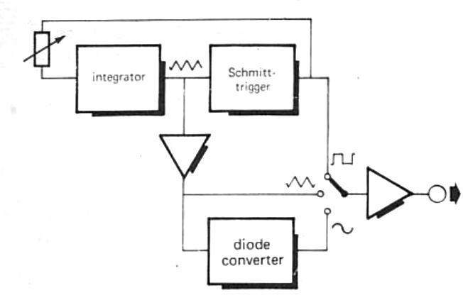
The circuit operating basics from the above shown block diagram. The function generator's main section is a triangle / square wave generator which consists of an integrator and a Schmitt trigger.
Once the output of the Schmitt trigger is high, the voltage feeding back from the Schmitt output to the input of the Integrator allows the output of the Integrator to ramp negative before it exceeds the lower output level of the Schmitt trigger.
At this stage the Schmitt trigger output is slow, so the small voltage fed back to the input of the integrator allows it to ramp up positively before the Schmitt trigger's upper trigger level is reached.
The Schmitt trigger's output goes high again, and the integrater output spikes negative again, and so forth.
The integrator output's positive and negative sweeps represent a triangular waveform whose amplitude is calculated by the Schmitt trigger's hysteresis (i.e. the difference between the high and low trigger limits).
The Schmitt trigger production is, naturally a square wave made up of alternating high and low output states.
The triangle output is supplied to a diode shaper through a buffer amplifier, that rounds off the highs and lows of the triangle to create an approximate to a sinewave signal.
Then, each of the 3 waveforms can be chosen by a 3-way selector switch S2 and supplied to an output buffer amplifier.
How the Circuit Works
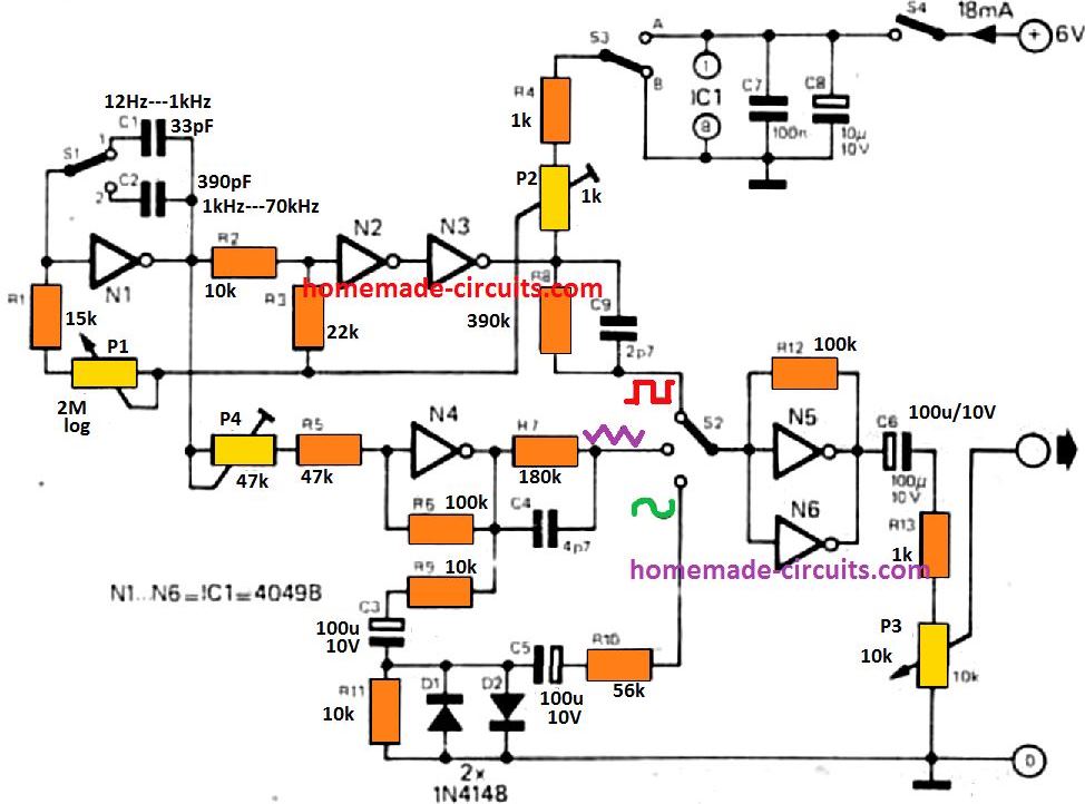
The full circuit diagram of the CMOS function generator as seen in the figure above. The integrator is entirely built using a CMOS inverter, N1, while the Schmitt mechanism incorporates 2 positive feedback inverters. It's N2 and N3.
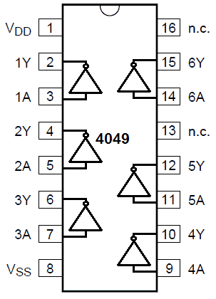
The following image shows the pinout details of the IC 4049 for applying into the above schematic
The circuit works this way; considering, for the moment, that the P2 wiper is in its lowest location, with N3 output being high, a current equivalent to:
Ub - U1 / P1 + R1
travels via R1 and p1, where Ub indicates the supply voltage and Ut the N1 threshold voltage.
Because this current is unable to move into the inverter high impedance input, it begins traveling towards C1/C2 depending on which capacitor is toggled in line by the switch S1.
The voltage drop over C1 thus decreases linearly such that the output voltage of N1 rises linearly before the lower threshold voltage of the Schmitt trigger is approached just as the output of the Schmitt trigger becomes low.
Now a current equivalent to -Ut / P1 + R1 flows through both R1 and P1.
This current always flows through C1, such that N1's output voltage increases exponentially until the Schmitt trigger's maximum limit voltage is achieved, the Schmitt trigger's output rises, and the entire cycle begins all over again.
To maintain the triangle wave symmetry (i.e. the very same slope for both the positive-going and the negative-going parts of the waveform) the condenser's load and discharge currents has to be identical, meaning Uj,-Ui should be identical to Ut.
However, sadly, Ut being decided by the CMOS inverter parameters, is normally 55% ! The source voltage Ub = Ut is approximately 2.7 V with 6 V and Ut approximately at 3.3 V.
This challenge is overcome with P2 which requires modification of the symmetry. For the moment, consider that thai R-is related to the positive supply line (position A).
Regardless of the setting of P2, the Schmitt trigger's high output voltage always remains 11.
Nevertheless, when N3 output is low, R4 and P2 establish a potential divider such that, based on P2's wiper configuration, a voltage between 0 V to 3 V could be returned back into P1.
This ensures the voltage is no longer -Ut and but Up2-Ut. In case the P2 slider voltage is around 0.6 V then Up2-Ut should be around -2.7 V, therefore the currents of charging and discharging would be identical.
Obviously, due to the tolerance in the value of Ut, the P2 adjustment should be performed to match specific function generator.
In situations in which Ut is less than 50 percent of the input voltage, connecting the top of R4 to ground (position B) might be appropriate.
A couple of frequency scales can be found, which will be assigned using S1; 12 Hz-1 kHz and 1 kHz to approximately 70 kHz.
Granular frequency control is given by P1 that changes the current of charge and discharge of C1 or C2 and thus the frequency through which the integrator ramps up and down.
The squarewave output from N3 is sent to a buffer amplifier via a waveform selector switch, S2, that comprises of a couple of inverters biased like a linear amplifier (hooked up in parallel to improve their output current efficiency).
The triangle wave output is provided through a buffer amplifier N4 and from there by the selector switch to the buffer amplifier output.
Also, the triangle output from N4 is added to the sine shaper, consisting of R9, R11, C3, Dl, and D2.
D1 and D2 pull little current up to around +/- 0.5 volts but their diverse resistance drops beyond this voltage and logarithmically limit the highs and lows of the triangle pulse to create an equivalent to a sinewave.
The sine output is transmitted to the output amplifier via C5 and R10.
P4, which varies the gain of N4 and hence the amplitude of the triangle pulse supplied to the sine shaper, changes the sinus transparency.
Too low a signal level, and the amplitude of the triangle would be below the threshold voltage of the diode, and it will proceed with no alteration, and too high a signal level, the highs and lows would be strongly clipped, thereby providing not well formed sine wave.
The output buffer amplifier input resistors are chosen such that all three waveforms have a nominal peak to minimum output voltage of around 1.2 V. The level of output could be changed through P3.
Setting Up Procedure
The adjustment method is simply to change the symmetry of the triangle and the purity of the sinewave.
In addition, the triangle symmetry is ideally optimized by examining the squarewave input, since a symmetrical triangle is produced if the squarewave duty cycle is 50% (1-1 mark-space).
To do this, you will have to adjust the preset P2.
In a situation where the symmetry increases as the P2 wiper is moved down towards the N3 output but correct symmetry could not be achieved, the upper part of R4 must be joined in the alternate position.
The purity of the sinewave is changed by adjusting P4 until the waveform 'looks perfect' or by varying for minimal distortion only if there is a distortion meter to check.
As the supply voltage affects the output voltage of the different waveforms, and therefore the purity of the sine, the circuit must be powered from a robust 6 V supply.
When batteries are used as power source batteries they should never be forced to run too much downward.
The CMOS ICs used as linear circuits drain higher current than in usual switching mode, and hence the supply voltage must not exceed 6 V, or else the IC can heat up due to heavy thermal dissipation.
Another great way of building a function generator circuit can be through the IC 8038, as I have explained below
2) Function Generator Circuit using IC 8038
The IC 8038 is a precision waveform generator IC specially designed for creating sine, square and triangular output waveforms, by incorporating least number of electronic components and manipulations.
Its working frequency range could be determined through 8 frequency steps, starting from from 0.001Hz to 300kHz, through the appropriate selection of the attached R-C elements.
The oscillatory frequency is extremely steady regardless of temperature or supply voltage fluctuations over a wide range.
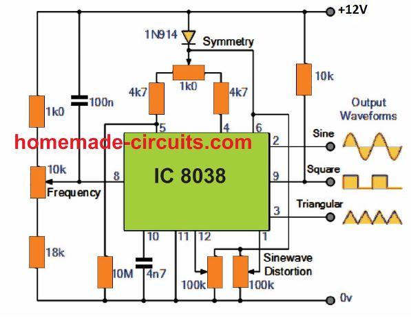
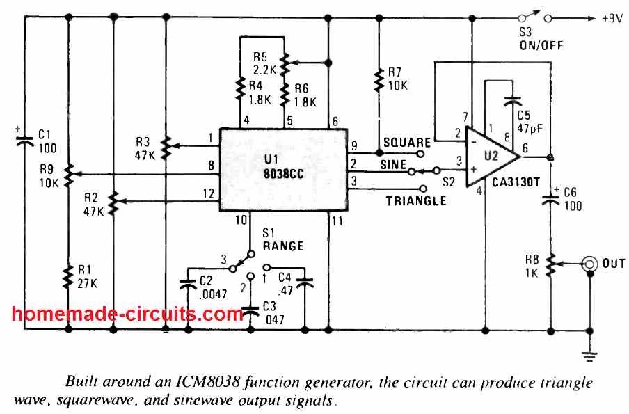
Additionally, the IC 8038 function generator offers a working frequency range up to as large as 1MHz. All the three fundamental waveform outputs, sinusoidal, triangular and square can be at the same time accessed through individual output ports of the circuit.
The frequency range of the 8038 can be varied through an external voltage feed, although the response may not be very linear. The proposed function generator also provides like adjustable triangle symmetry, and adjustable sine wave distortion level.
3) Function generator Using IC 741
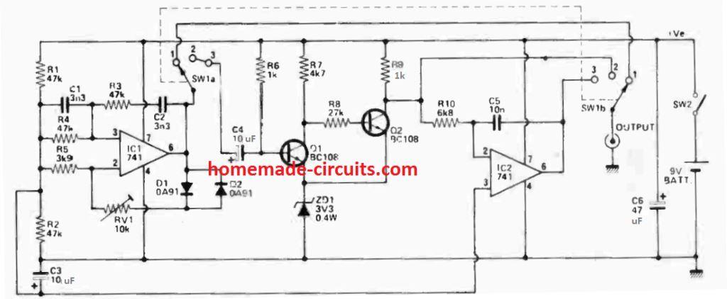
This IC 741 based function generator circuit delivers increased test versatility compared to the typical sine wave signal generator, giving 1 kHz square and triangle waves together, and it is both low-cost and very simple to construct.
As it appears the output is approximately 3V ptp on square wave, and 2V r.m.s. in the sine -wave. A switched attenuator might quickly be included if you want to be gentler to the circuit that's being tested.
How to Assemble
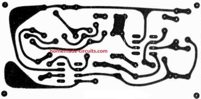
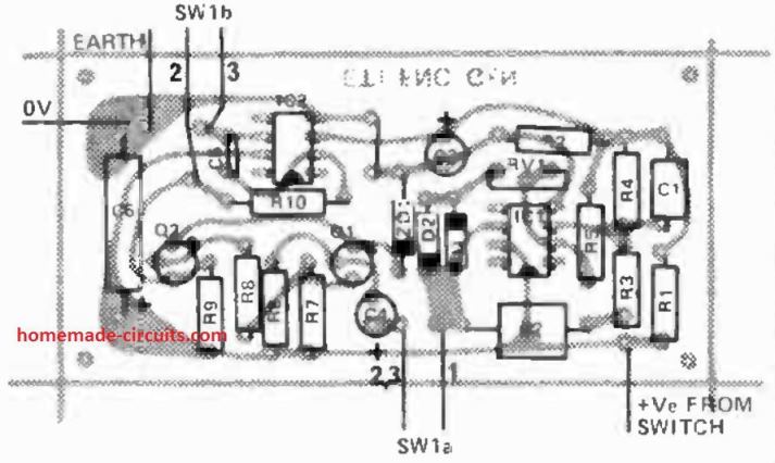
Start stuffing the parts onto the PCB as displayed in the component layout diagram, and make sure to insert the polarity of the zener, electrolytics and ICs correctly.
How to Set up
To set up the simple function generator circuit, just fine-tune RV1 until the sine waveform is slightly under the clipping level. This provides you with the most effective sinewave through the oscillator. The square and triangle do not require any specific adjustments or set ups.
How it Works
- In this IC 741 function generator circuit, the IC1 is configured in the form of a Wien bridge oscillator, operating at 1 kHz frequency.
- Amplitude control is supplied by the diodes D1 and D2. The output from this IC is driven via either to the output socket or to the squaring circuit.
- This is connected to SW1a by means of C4 and it is a Schmidt trigger (Q1 -Q2). The zener ZD1 works like a 'hysterisis-free' trigger.
- The IC2, C5 and R10 integrator generates the triangular wave from the input square wave.
4) Simple UJT Function Generator
The unijunction oscillator shown below, is among the easiest sawtooth generators. The two outputs of this give, namely, a sawtooth waveform and a sequence of trigger pulses.
The wave ratchets up from around 2V (the point of the valley, Vv) to the maximum peak (Vp).
The peak point relies on the power supply Vs and the stand-off BJT ratio, which may range from about 0.56 to 0.75, with 0.6 being a common value. The period of one oscillation is roughly:
t = - RC x 1n[(1 - η) / (1 - Vv/Vs)]
where ‘1n’ indicates natural logarithm usage. Considering standard values, Vs = 6, Vv = 2, and η = 0.6, the above equation simplifies to:
t = RC x 1n(0.6)
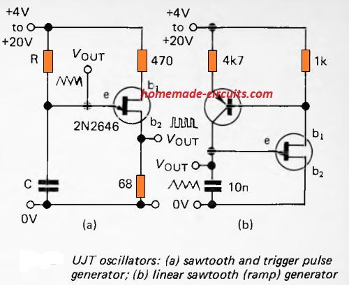
Since capacitor charging is incremental, the sawtooth 's increasing slope isn't linear. To many Audio applications, this barely matters. The Figure (b) demonstrates the charging capacitor via a constant-current circuit. This enables the slope going straight up.
The capacitor's charge rate is now constant, independent from Vs, although Vs still influences the peak point. Since the current is dependent on transistor gain, there is no simple formula for frequency measurement. This circuit is designed to work with low frequencies, and has implementations as a ramp generator.
5) Using LF353 op amps
Two op amps are used to construct a precise square wave and triangle wave generator circuit. The LF353 set includes two JFET op amps which are best suited for this application.
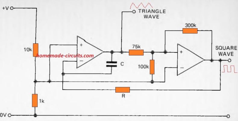
The output signal frequencies are calculated by the formula f=1 / RC. The circuit shows an extremely wide operating range with hardly any distortion.
R may have any value between 330 Ohm and around 4.7 M; C can be of any value from around 220pF to 2uF.
Just like the above concept, two op amps are used in the next sine wave an cosine wave function generator circuit.
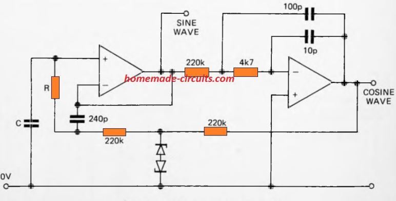
They generate nearly identical frequency sine wave signals but 90 ° out of phase, and therefore output of the second op amp is termed as a cosine wave.
Frequency is affected by the collection of acceptable R and C values. R is in the 220k to 10 M range; C is between 39pF and 22nF. The connection between R, C and/or is a bit complex, as it must reflect the values of other resistors and capacitors.
Use R = 220k and C = 18nF as an initial point that provides a frequency of 250Hz. The Zener diodes can be low power output diodes of 3.9V or 4.7V.
6) Function Generator using TTL IC
A couple of gates of a 7400 quad two-input NAND gate constitutes the actual oscillator circuit for this TTL function generator circuit.
The crystal and a adjustable capacitor works like the feedback system across the input of gate U1-a and the output of gate U1-b. Gate U1-c functions like a buffer between the oscillator stage and the output stage, U1-d.
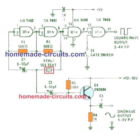
Switch S1 acts like a manually switchable gate control to toggle the squarewave output of U1-d at pin 11 ON/OFF. With S1 open, as indicated, the square-wave is generated at the output, and once closed the equare waveform is switched off.
The switch could be substituted with a logic gate to digitally command the output. An almost ideal 6- to 8-volt peak-to-peak sine wave is created at the connecting point of of C1 and XTAL1.
The impedance on this junction is very high and is unnable to provide a direct output signal. Transistor Q1, set up as an emitter-follower amplifier, supplies a high input impedance to the sine-wave signal and a low output impedance to an outside load.
The circuit will crank up almost all types of crystals and will run with crystal frequencies of below 1 MHz to above 10 MHz.
How to Set Up
Setting up this simple TTL function generator circuit can be quickly initiated with the following points.
If there's an oscilloscope available with you, hook it up to the square-wave output of U1-d on pin 11 and position C1 in the center of the range that delivers the most effective output waveform.
Next, observe the sine-wave output and adjust C2 for getting the finest looking waveform. Return to C1 control knob and fine-tune it to and fro a bit until the most healthy sine-wave output is achieved on the scope screen.
Parts List
RESISTORS
(All resistors are -watt, 5% units.)
RI, R2 = 560-ohm
R3 = 100k
R4 = 1k
Semiconductors
U1 = IC 7400
Q1 = 2N3904 NPN silicon transistor
Capacitors
C1, C2 = 50 pF, trimmer capacitor
C3, C4 = 0.1 uF, ceramic-disc capacitor
Miscellaneous
S1 = SPST toggle switch
XTAL1 = Any Crystal (see text)
7) Crystal Controlled Best Sine waveform Circuit
The following waveform generator, is a two-transistor, crystal oscillator circuit that performs superbly, cheap to build, and requires no coils or chokes.
The price depends primarily on the crystal used, as the overall cost of the other elements must be hardly a few dollars. Transistor Q1 and the several adjacent parts form the oscillator circuit.
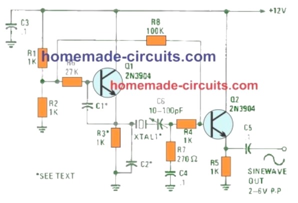
The ground path for the crystal is directed by means of C6, R7, and C4. In the C6 and R7 junction, which is a pretty small impedance position, the RF is applied to an emitter-follower amplifier, Q2.
The waveform shape at the C6/R7 junction is really an almost perfect sine wave. The output, at the emitter of Q2 ranges in amplitude from around 2- to 6-volts peak-to-peak, based upon on the Q factor of the crystal's and the capacitors C1 and C2 values.
The C1 and C2 values decide the frequency range of the circuit. For crystal frequencies under 1 MHz, C1 and C2 ought to be 2700 pF (.0027 p,F).
For frequencies between 1 MHz and 5 MHz, these can be 680-pF capacitors; and for 5 MHz and 20 MHz. you can apply 200-pF capacitors.
You could possibly try testing with values of those capacitors to get the finest looking sine wave output. Additionally, the adjustment of capacitor C6 can have an effect on the two output level and the overall shape of the waveform.
Parts List
RESISTORS
(All resistors are -watt, 5% units.)
R1-R5-1k
R6-27k
R7-270-ohm
R8-100k
CAPACITORS
C1,C2—See text
C3,C5-0.1-p.F, ceramic disc
C6-10 pF to 100 pF, trimmer
SEMICONDUCTORS
Q1, Q2-2N3904
XTAL1—See text
Sawtooth Generator Circuit
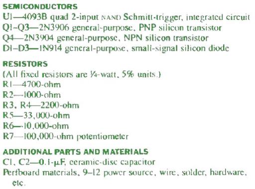
In the sawtooth generator circuit, the parts Q1, D1-D3, R1, R2, and R7 are configured like a simple constant-current generator circuit which charges capacitor C1 with a constant current. This constant charging current creates a linear increasing voltage over C1.
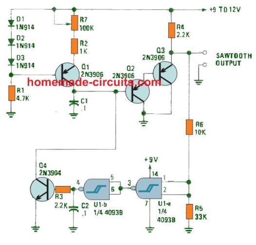
Transistors Q2 and Q3 are rigged like a Darlington pair to push the voltage through C1, to the output with no loading or distorting effects.
As soon as the voltage around C1 increases to around 70% of the supply voltage, gate U1-a activates, triggering the U1-b output to go high and briefly switch on Q4; which continues to be ON while capacitor C1 discharges.
This finishes a single cycle and initiates the next. The circuit's output frequency is governed by R7, which supplies a low-end frequency of approximately 30 Hz and an upper-end frequency of around 3.3 kHz.
The frequency range could be made higher by decreasing the value of C1 and dropped by increasing the C1's value. To preserve Q4's peak discharge current under control. C1 should not be bigger than 0.27 uF.
Parts List
8) Function Generator Circuit using a Couple of IC 4011
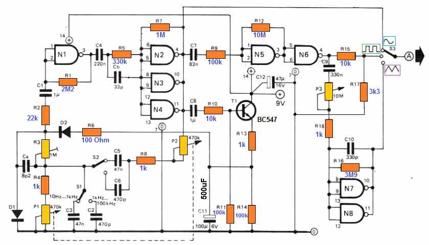
The foundation of this circuit is actually a Wien -bridge oscillator, which offers a sine wave output. The square and triangular waveforms are subsequently extracted out of this.
The Wien -bridge oscillator is constructed using a CMOS NAND gates N1 to N4, while the amplitude stabilization is supplied by transistor T1, and diodes D1 and D2.
These diodes possibly, must be matched up set of two, for lowest distortion. The frequency adjusting potentiometer P1 must also be a high-quality stereo potentiometer with internal resistance tracks paired to inside 5% tolerance.
The preset R3 gives adjusting facility for least distortion and in case matched up parts are employed for D1, D2 and P1 the overall harmonic distortion could be under 0.5%.
The output from the Wien -bridge oscillator is applied to the input of N5, which is biased into its linear region and functions as an amplifier. NAND gates N5 and N6 collectively enhance and clip the oscillator output to generate a square waveform.
The duty -cycle of the waveform is relatively influenced by the threshold potentials of N5 arid N6, however it is in close proximity to 50%.
The gate N6 output is supplied into an integrator built using the NAND gates N7 and N8, that harmonizes with the square wave to deliver a triangular waveform.
The triangular waveform amplitude is, for sure is dependent on the frequency, and as the integrator is simply not very accurate the linearity additionally deviates with respect to the frequency.
In reality the amplitude variation is actually pretty trivial, considering that the function generator will often be used together with a millivoltmeter or an oscilloscope and the output could be easily checked.
9) Function Generator circuit using LM3900 Norton Op Amp
A extremely handy function generator that will reduce hardware and also the price could be constructed with a single Norton quad amplifier IC LM3900.
If resistor R1 and capacitor C1 are removed out of this circuit, the resulting setup will be the common one for a Norton-amplifier square-wave generator, with the timing current entering capacitor C2. The inclusion of an integrating capacitor C1 to the square-wave generator creates a realistically precise sine wave at the output.
Resistor R1, that facilitates to complement the circuit's time constants, enables you to adjust the output sine wave for lowest distortion. An identical circuit enables you to put in a sine-wave output to the standard hookup for a square-wave/triangular-wave generator designed with two Norton amplifiers.
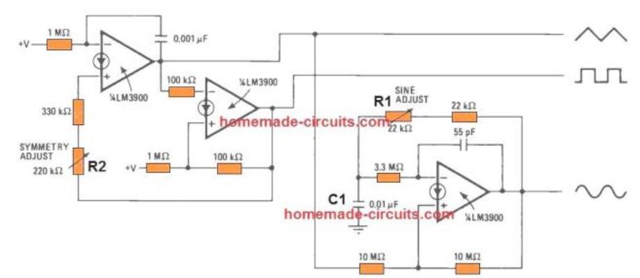
As demonstrated in the picture triangular output works like the input for the sine -shaper amplifier.
For the part values provided in this article, the circuit's running frequency is approximately 700 hertz. Resistor R1 can be used for adjusting lowest sine -wave distortion, and resistor R2 can be used for adjusting the the symmetry of the square and triangular waves.
The 4th amplifier in the Norton quad package could be hooked up as an output buffer for all 3 output waveforms.
10) Function Generator using IC 566
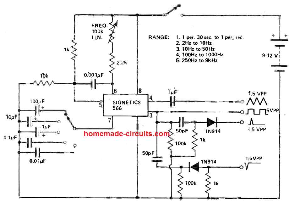
The IC 566 becomes ideally suited for building a test generator with the help of its internal voltage controlled oscillator (VOC).
The circuit is designed supply individual outputs offering triangular and square waves along with a set of positive and negative going spike outputs.
The amplitude of the square wave is 5 V pk-pk, the remaining waveforms are 1.5 V pk-pk. Frequency depends upon the capacitor value which is attached to pin 7 of the IC.
It is advised to make use of tantalum capacitors instead of electrolytics. The outputs of this IC 566 function generator are created to handle high impedance loads. A transistor buffer stage is necessary to complement to low input impedance equipment.
Spot Sine wave Function Generator
The next figure illustrates a circuit that uses an IC 7556 as an integrator.
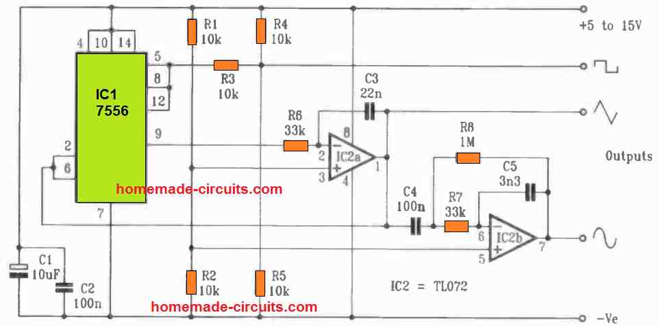
When the integrator is fed with a square wave input from the timer, it converts it to a triangular wave. When the triangle-wave signal is applied into another integrator, it is transformed into a sine wave.
With a very basic circuit, this method may be utilized to create a pretty clean sine wave of a set frequency. All three fundamental waveforms, square, triangle, and sinewave, are generated with almost identical peak-to-peak voltage amplitudes in this version.
The amplitude of the sinewave, 3 volts peak-to-peak with a 9 V supply, is nearly comparable to one volt RMS, which is a useful quantity for audio testing.
The goal of this spot sinewave generator is to make all three outputs with about the identical output voltage so that other circuits may be quickly tested for responsiveness to varied waveforms. With a peak-to-peak voltage of one-third of the supply, the triangle wave defines the starting value.
The square wave originally possesses the supply voltage value as it varies from rail to rail, although it is attenuated to nearly the required value by means of the two resistors R4 and R5. These two resistors could be removed if they are not necessary. The input of lC2b, a second integrator, is linked to the triangle wave.
Due to input offset voltages and currents, etc., the output of an integrator might finally drift as much as it can towards one of the supply rails unless some form of DC feedback is used.
Therefore lC2b is AC coupled to the input signal via C4 and the large feedback resistor R8, holds the right DC output level.
The levels of these two components are adequate to prevent signal distortion at the operational frequency.
The settings of R7 and C5 adjust the output amplitude to the desired level of roughly one-third of the supply peak-to-peak. the frequency is determined. by the formula:
f = 1 / 1.333 x R6 x C5
This method produces a pretty nice sinewave, with the sole downside being that the frequency cannot be readily changed.
Any change in the input frequency to the second integrator will necessitate a change in the values of RT and C5 in order to keep the right sinewave output amplitude, and there is no quick method to achieve this.
Simple Function Generator Circuit using IC 555
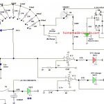
If you are having a single spare IC 555and some passive electronic parts then you can quickly build this useful little function generator circuit.
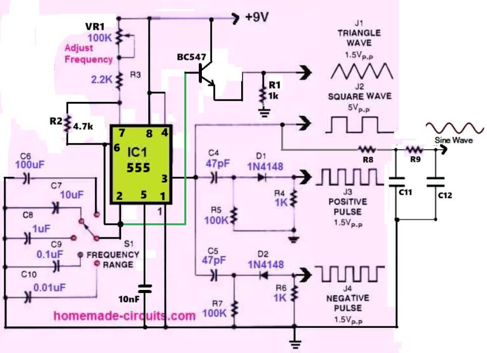
As can be seen in the figure above, the IC 555 can be used to generate 5 useful waveforms.
It can generate triangle wave, square wave, train of positive pulse and a train of negative pulse, and also sine waveform.
Switch S1 can be used for selecting the frequency range, while the pot VR1 can be used for adjusting the frequency output of the 555 IC outputs.



Comments
Hi
I am trying to assembly the circuit using Ne556
But the one you attached has only 8 pin while 556 has 16pin
do you mean 555 instead
Thank 3
Hi, Yes, it looks like it is a 555 configuration, but strangely pin#4 is not connected to the positive so i am not sure how the circuit can work.
Can you please simulate the circuit on this simulator, and check the response. This circuit was designed by an external author.:
hi, can these circuits be operate using dc input voltage? which will be the best suitable for it? as I’m building a singular project of function generate, i want to power it through dc battery
Hi, yes, all these circuits can be operated with DC sources like batteries…
In the circuits “Simple UJT Function Generator” circuits, B2 should be tied to positive
and B1 tied to ground.
Yes, that’s right!
dude, have i try function generator cmos 4049 ? there’s an error in your schematic. It wont work, the c for range frequency connected to wrong point.
Hello Swagatam I really enjoy your explanations, I am a beginner, please explain to me how to increase the RF
signal that gives between 1GHz to 6GHz, In other words, what should I add or subtract from these components?
Best regards
Thank you Adam, I appreciate your kind words!
I am actually not sure how to convert one of these to handle GHz frequencies. According to me none of the above designs can be modified to generate GHz range…
Hi, please specify which exact position you are referring to in the first diagram, I will try to correct it soon…
junction capacitor 33n and 390 pf should connected to input gate N2, tyhis common for 4049 or 4069 oscillator, because it wasnt schmitt trigger not gate type.
Ok, thanks for the update, in that case we can simply replace the 4049 IC with a CD40106B.
I need a low out put single frequency of old Schumann 7.8 Hz as sine wave. powered by regulated 6volt or 5V DC for some low budget research. ASAP Thanks
I have an article on sinewave generator circuits. You can check it out in the link below. I hope it helps you to get the required circuit:
https://www.homemade-circuits.com/simple-sine-wave-generator-circuits/
Can you please provide a pcb layout for no. 2 ( ic8038 based) circuit. Also please explain the role of opamp in this circuit.
Sorry, I do not have a PCB design for the 2nd circuit, if possible I will try to update it.
I need a linear rise and fall times not exponential. The RC circuit won’t do that.
Thanks for your reply
Processing an existing pulse looks difficult, however if you want to generate a triangle wave with adjustable slope then that may be possible.
I need a simple circuit which can control the rising and falling slope of a pulse signal. If you can contribute or any of your followers, I will appreciate it.
I think that can be done with a simple RC network.
dear sir. I have been into ghost research since 1970, and have been using all the old school methodes ever since, however i have decided to go forward with the new stuff thats out there, however, living in england it is very hard to obtain components off the shelf (as in the u.s. you can get it all) or at elect shops. I want to make a ramp genny or get a circuit that has at least 0 to 8v+ voltage for tuning of radio front ends. I also cannot get the u.s. part NTE 618 v.c. diode, (a link for this device to buy would be awsome) as i cannot get it here in the u.k. I am myself an electronic engineer and radio ham (g7gna) i would like to thank you for all that you have done to help others like myself. BE SAVE. and thank you lenny (g7gna)
Dear Lenny, you can get electronic parts from any online electronic spare part store, there are plenty of them.
You just have to Google the phrase: “Buy electronic components” and you will be be able to find many stores, you can simply select one of them as per your choice.
Please I need the full project soft copy material for the topic design and development of function generator using CD4049
Thanks
This is another circuit I have studied and considering building, some for a multiple function generator with numerous outputs of various wave forms simultaniously. I just have a question about 2 caps in the TTL version. The text indicates .1 Pf but I think they should be .1 Ufd. Which is correct in your opinion? The schematic appears to refer to .1 Uf caps and in my opinion this would be logical as C4 would be for transients from the 7805 that is indicated with the 12-16 Vdd connected to the collector of the 2n3904 and the capacitor connected to the emitter of same Q, C3. Would you kindly send me a message please. In the mean time I will go with the Uf and test.
You are absolutely correct, I have updated the cap values accordingly. yes the functions of the relevant parts as explained by you is also correct.
That’s cool and again, I can’t believe how fast you got back and as far as I can say, I think it is amazing how you keep up with everything you are doing. I have been reading and following your stuff now for almost 15 years.
Thanks so much! Appreciate greatly for being a dedicated member of his site and reading my articles since so long 🙂