A sinewave inverter using class-D amplifier functions by converting a small sinewave input frequency into equivalent sine PWMs, which is finally processed by an H-bridge BJT driver for generating the mains sinewave AC output from a DC battery source.
What is Class-D Amplifier
The working principle of a class-D amplifier is actually simple yet extremely effective. An input analogue signal such as an audio signal or a sinusoidal waveform from an oscillator is chopped into equivalent PWMs also called SPWM.
These sine equivalent PWMs or SPWMs is fed to a power BJT stage, where these are amplified with high current, and applied to the primary of a step up transformer.
The transformer finally transforms the sine equivalent SPWM into 220V or 120V sine wave AC, whose waveform is exactly in accordance with the input sine wave signal from the oscillator.
Advantages of Class-D Inverter
The main advantage of a class-D inverter is its high efficiency (almost 100%) at a reasonably low cost.
Class-D amplifiers are easy to build and set up, which enables the user to produce efficient, high power sine wave inverters quickly without many technical hassles.
Since the BJTs have to work with PWMs, it allows them to be cooler and more efficient, and this in turn allows them to work with smaller heatsinks.
A Practical Design
A practical class-D inverter circuit design can be witnessed in the following diagram:
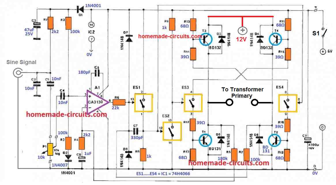
The working of the pwm class-D inverter is fairly simple. The sine wave signal is amplified by the op amp A1 stage to adequate levels for driving the electronic switches ES1---ES4.
The electronic switches ES1---ES4 open and close causing rectangular pulses to be generated across the bases of the transistors T1---T4 bridge alternately.
The PWM or the width of the pulses is modulated by the input sine signal resulting in a sine equivalent PWMs fed to the power transistors,and the transformer, ultimately producing the intended 220V or 120V sine-wave mains AC at the output of the transformer secondary.
The duty factor of a rectangular signal produced from the ES1---ES4 outputs is modulated by the amplitude of the amplified input sine wave signal, which causes an output switching SPWM signal proportional to the sine wave RMS. Thus the on-time of the output pulse is in accordance with the instantaneous amplitude of the input sine signal.
The switching period interval of the on-time and the off -time together determines the frequency which will be constant.
Consequently, a uniformly dimensioned rectangular signal (square wave) is created in the absence of an input signal.
As a way to achieve fairly good sine wave at the output of the transformer, the frequency of the rectangular wave from ES1 should be at the very least two times as high as the highest frequency in the input sine signal.
Electronic Switches as amplifiers
The standard working of the PWM amplifier is implemented by the 4 electronic switches made around ES1---ES4. Supposing that the input of the op amp input at the zero level, causes the capacitor C7 to charge via R8, until the voltage across C7 attains the level that is sufficient to switch ON ES1.
ES1 now closes and begins discharging C7 until its level drops below the switch ON level of ES1. ES1 now switches OFF initiating the C7 charging again, and the cycle rapidly turns ON/OFF at a rate of 50 kHz, as determined by the values of C7 and R8.
Now, if we consider the presence of a sine wave at the input of the op amp, it effectively causes a forced variation on the charge cycle of C7, causing the ES1 output PWM switching to get modulated as per the rise and fall sequence of the sine wave signal.
The output rectangular waves from the ES1 now produces SPWM whose duty factor now varies in accordance with the input sine signal.
This results in a sine wave equivalent SPWM to be alternately switched across the T1---T4 bridge, which in turn switches the transformer primary to generate the required AC mains from the secondary wires of the transformer.
Since the secondary AC voltage is created in accordance with the primary SPWM switching, the resultant AC is a perfectly equivalent sine wave AC of the input sine signal.
Sine wave Oscillator
As discussed above, the class-D inverter amplifier will need a sine wave signal input from a sine wave geneartor circuit.
The following image shows a very simple single transistor sine wave generator circuit which can be effectively integrated with the PWM inverter.
The frequency of the above sine wave generator is around 250 Hz, but we will need this to be around 50 Hz, which can be changed by altering the values of C1---C3, and R3, R4 appropriately.
Once, the frequency is set, the output of this circuit could be linked with the C1, C2 input of the inverter board.
PCB Design and Transformer Wiring
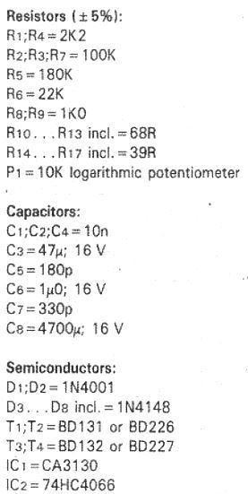
Parts List
Transformer: 0-9V/220V current, will depend on the transistors wattage and battery Ah rating
Specifications:
The proposed class-D PWM inverter is a small 10 watt test sample prototype. The 10 watt low output is due to the use of low power transistor for T1---T4.
The power output can be easily upgraded to 100 watts by replacing the transistors with TIP147/TIP142 complementary pairs.
It can increased to even higher levels by using higher BUS DC line for the transistors, anywhere between 12V and 24V


Comments (37)
Hi I am retired and from South African with load shedding. I try to build a pure sine wave inverter of around 3Kw with the stuff that is laying around. I got the first part with the sine wave and MOSFET working and the signal and hertz is correct. I have centre tap transformers from a square wave inverter and want to know if I can use that with sine wave. My tries so far blown a lot of MOSFETs.
Please help with a solution.
Regards
Hi, Yes you can use the center tap transformer as long as it is correctly rated for your MOSFETs and the battery voltage.
Please I need a help on, to step down 220v to 100v.
Because power supply in our area is 220v, but I have a transformer that requires 100v????
There’s no easy way to do this. Instead you should change the transformer.
Maybe I will try using my variable stabilizer to do that thanks
OK, good!
with a low frequency inverter, is it possible to use a center tap output transformer to get a split phase type output as we use in North America (ie L1-L2 230v and L1-CT / L2-CT 115v)
If this is possible, is it possible to balance the output lets?
Thanks again for any advice you might be able to give.
Take care
Doug
Yes it is possible to use a center tap at the secondary side of an inverter transformer to create a split phase AC output. The center tap becomes the neutral and the two outer wires act like the phase (LIVE) outputs. The two phase outputs can be balanced by connecting similar loads across the two phase outlets and the common center tap neutral.
Hi and thank you for all the inverter designs. I have build i thew and they work great. You don’t by any change have an H-bridge design working with the PWM board EGS002. The reason for my question is that i have build using the EGS002 with a 12vdc/240vac transformer. But i only get around 150vac . As soon as i try to increase my voltage via a variable resistor the EGS002 shuts down beacuse of “undervoltage” i like using the EGS002 because i get a beautifull signwave, at 50hz with a 50% duty cycle.
Again thank you.
Regards
Peter
Hi, thanks, and glad you could make the above designs successfully.
Sorry, I have not yet built an EGS002 based inverter, so would be difficult for me to solve your problem…
OK, thanks.
if the 220 vac from the net goes off, the inverter still produce 220 vac through the battery and the 5 Vac from the transformer is still generated and applied to the inverter input… It seems to be a dog that eats its tail ! Will you please clarify ? Thanks for all.
Regards, iw2fvo.
Hi Swagatam,
I have changed C1 & C4 to 470nF. A1 does not trigger with this combination, however if I hardwire C4 then A1 triggers, but still no PMW. I have disconnected R5 & R7. Also no PMW. I have tried different values for C5, C6, C7, R2, R3 & R4. Still no PMW & only rectangular wave forms. Is there not an alternative cct that I can use to produce the required PWM?
Your assistance will be much appreciated.
Regards
Jan
Hi jan, the above design was originally an audio amplifier which was modified into an inverter by me. You can find the original design in the following article:
https://www.homemade-circuits.com/4-efficient-pwm-amplifier-circuits-explained/
Hi Jan, in all audio amplifiers we have a capacitor at the input sides, and the audio signal easily pass through them, so in this circuit also the presence of C1, and C4 should not pose any problems. I believe the circuit is tested and therefore the PCB had been finalized for this design. Are you using the same PCB as shown in the last image? In the original design the whole circuit was operated at 6V, so you try that also.
Actually I am not sure about the inverter output in the absence of an input grid sinewave signal….it seems it might keep generating the base rectangular frequency at the output.
In that case we can apply a circuit for detecting a square wave and trip the inverter off
However, in GTI is the inverter supposed to continue applying the AC into the grid line, when grid AC fails? or shut down?
thanks,
regulations requre that the there will not be any output from the inverter if the main grid fails.
iw2fvo
OK, that makes things a bit easier. The square wave RMS from the inverter should be slightly lower than the sinewave RMS, this can be used for the detection of the grid AC presence or absence through an op amp, and for switching off inverter during a mains failure…
Hi Swagatam, in the description of the circuit you talk about MOSFET transistors, but in the diagram BJT transistors are used, it would be a good idea to publish the circuit with MOSFETs since the values of some components will have to change. Greetings from Argentina.
Thank you Beto for indicating the mistake, I’ll correct it soon by replacing the MOSFET with BJTs.
Actually I am not quite sure how the BJTs could be replaced here with FETs due to strange arrangement of the resistive dividers across the bases of the BJTs. This arrangement may work with the shown BJTs but may not with FETs.
This will need to be experimented the wiring to exactly know how the MOSFETs could be used.
how could I make this project a GRID TIE inverter please ?
Thanks
you could take a stepped down 5V 100Hz grid sample from a bridge rectifier and feed it to the input of the inverter and then configure the transformer output with the grid wiring….be sure to be extremely careful with the procedures, since the concept is only as per my assumptions and is not verified
Thanks for the reply,
>100 Hz is the double of the grid freq… is it OK?
>If the grid goes down , the invertyer must shut down: how to do it ?
Regards,
OK i that case you can connect the 5V AC source directly across the input…this could be from a small 220/120V to 4.5 V / 500 mA transformer.
Hi Swagatam,
I am confused now. I am getting a Square wave signal out of A1-6. Is that correct?
Is A1-6 also PWM or just a amplified Sine Wave.
If I can not get this to work can you suggest an alternative cct to replace A1 side of the cct and then interface remainder of the cct ie. ES1 – ES4
A1-6 is the sine amplified output, not PWM.
you can try the following alternate concept, which has been tested by me:
Apply the sine wave to pin#5 of IC2
THe N1—N6 can be removed, and the transistors can be directly hooked up with the pin#3 of the IC2.
The motor can be replaced with the transformer primary
Hi Jan, ES1 is the main sine PWM generator, while the other switches are buffers only, so yes, you should get varying PWMs at the output of ES1. Normally when there’s no sine wave at the input, the output from ES1 will be producing 50 kHz rectangular waves, but as soon as a sine wave is detected, the square waves become modulated by the sine waveforms and we get SPWM at the outputs of the ES1—ES4.
Hi Swagatam,
I need the inverter to handle a 160W load. Can you please suggest a BJT pair that I can use to achieve this? I will be using 12V to power the circuit.
Regards
Jan
Thank you Swagatam,
I really appreciate your assistance.
Best regards
No problem Jan!
Thank you for your reply.
I have checked it with my scope and it is definitely not PWM signal.
I do get my sine wave out of A1-6 and into ES1-13.
On ES1-1 I get a rectangular signal. It should be PWM correct?
C7 is the only component which will produce the PWM signal?
So I am just wondering if it is not the feedback R7 causing the problem. Can I disconnect R7 without blowing anything up to see if I then get PWM?
The PWMs should be available at ES3, and ES4, but I think the input capacitors are crucial, C1 and C4 cannot be replaced with wire links. The feedback is only for output voltage control, it is not related to sine PWM generation. But you can remove the feedback just to check what results it produces.
Hi Swagatam,
I have built this circuit. First of all I had to bypass C1 & 4 to get A1 to trigger with the 50Hz signal from Sine Wave Generator. Everything else seems to work fine, except that the primary output to the transformer is a square wave signal instead of a AC sine wave. Can you please suggest what I should check?
Regards
Jan
Hi Jan, I don’t think bypassing the input capacitors would be correct, instead you can try the increasing the values to 0.47uF.
The output will be rectangular wave but modulated in accordance with the sine wave, meaning the output rectangular waves will slowly create wider PWMs as the sine wave amplitude increases and then the PWM will get narrower as the sine wave amplitude comes down or decreases.
You will need an oscilloscope to check this..
Thank you for your reply. Does that mean that we now don’t have to use D3 – D6.
I forgot to show them in the diagram, they will still be required to protect the transistors against transformer back emfs.
Hi Jan, You can try TIP35 and TIP36 pairs, and connect them with the existing BD132 and BD131 transistors as Darlington pairs, as shown below: