Bootstrapping is a crucial aspect that you will find in all H-bridge or full bridge networks with N-channel mosfets.
It is a process in which the gate/source terminals of the high side mosfets are switched with a voltage that's at least 10V higher than its drain voltage. Meaning, if the drain voltage is 100V, then the effective gate/source voltage must be 110V in order to enable the full transfer of the 100V from the drain to the source of the high side mosfet.
Without bootstrapping facility an H-bridge topology with identical mosfets simply won't work.
We will try to understand the details through a step by step explanation.
A bootstrapping network becomes necessary only when all the 4 devices in the H-bridge are identical with their polarity. Commonly these are n-channel mosfets (4 p-channel is never used due to obvious reasons).
The following image shows a standard n-channel H-bridge configuration
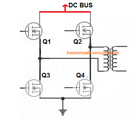
The main function of this mosfet topology is to switch the "load" or the transformer primary in this diagram, in a flip-flop manner. Meaning, to create an alternating push-pull current across the connected transformer winding.
To implement this the diagonally arranged mosfets are switched ON/OFF simultaneously. And this is cycled alternately for the diagonal pairs. For instance the pairs Q1/Q4 and Q2/Q3 are together switched ON/OFF, alternately. When Q1/Q4 is ON, Q2/Q3 is OFF, and vice versa.
The above action forces current to alternately change its polarity across the connected transformer winding. This in turn causes the induced high voltage across the secondary of the transformer also to change its polarity, producing the intended AC or alternating output on the secondary side of the transformer.
What are High-Side Low-Side Mosfets
The upper Q1/Q2 are called the high side mosfets, and the lower Q3/Q4 are called the low side mosfets.
The low side mosfet have their reference leads (source terminals) appropriately connected with the ground line. However the high side mosfet have no access to the reference ground line directly, instead are connected to the transformer primary.
We know the "source" terminal of a mosfet or the emitter for a BJT must be connected to the common ground line (or the common reference line) in order to enable it to conduct and switch a load normally.
In an H-bridge since the high side mosfets are unable to access the common ground directly, switching them ON effectively with a normal gate DC (Vgs) become impossible.
This is where the problem arises, and a bootstrapping network becomes crucial.
Why this is a Problem?
We all know that a BJT requires a minimum 0.6V between its base/emitter to conduct fully. Similarly, a mosfet requires around 6 to 9V across its gate/source to conduct fully.
Here, "fully" means optimal transfer of the mosfet drain voltage or the BJT collector voltage to their respective source/emitter terminals, in response to gate/base voltage input.
In an H-bridge the low side mosfets have no problems with their switching parameters and these can be switched normally and optimally without any special circuitry.
This is because the source pin is always at zero or ground potential allowing the gate to be elevated at the specified 12V or 10V above the source. This meets the required switching conditions of the mosfet and allows it to pull the drain load to ground level fully.
Now, observe the high side mosfets. If we apply 12V across its gate/source, the mosfets initially responds well and begins conducting the drain voltage towards the source terminals. However, while this happens, due to the presence of the load (transformer primary winding) the source pin begins experiencing a rising potential.
When this potential rises over 6V, the mosfet begins stalling, because it has no more "space" to conduct, and by the time the source potential reaches 8V or 10V the mosfet just stops conducting.
So I have explained this with the help of the following simple example.
Here the load can be seen connected at the source of the mosfet, imitating a Hi-side mosfet condition in an H-bridge.
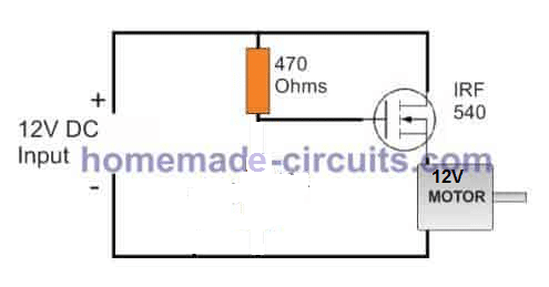
In this example if you measure the voltage across the motor you will find it to be just 7V, although 12V is applied at the drain side.
This is because the 12 - 7 = 5V is the bare minimum gate/source or Vgs that's being utilized by the mosfet to keep the conduction ON. Since the motor here is a 12V motor it still rotates with the 7V supply.
If suppose we used a 50V motor with 50V supply on the drain and 12V on the gate/source, we may see just 7V on the source, producing absolutely no movement on the 50V motor.
However, if we apply around 62V across the gate/source of the mosfet. This would instantly turn ON the mosfet, and its source voltage would rapidly start rising until it reaches to the maximum 50V drain level.
But even at 50V source voltage, the gate being 62V would be still 62 - 50 = 12V higher than the source, enabling a full conduction of the mosfet and the motor.
This implies, the gate source terminals in the above example would require something around 50 + 12 = 62V to enable a full speed switching on the 50V motor.
Because this allows the gate voltage level of the mosfet to be properly elevated at the specified 12V level above the source.
Why doesn't the Mosfet Burn with such high Vgs
It's because as soon as the gate voltage (Vgs) is applied, the drain side high voltage is instantly switched ON and it rushes at the source terminal cancelling the excess gate/source voltage. Finally, only the effective 12V or 10V is rendered at the gate/source.
Meaning, if 100V is the drain voltage, and 110V is applied on the gate/source, the 100V from drain rushes at the source, nullifying the applied gate/source potential 100V, allowing only the plus 10V to operate the procedures. Therefore the mosfet is able to operate safely without burning.
What is Bootstrapping
From the above paragraphs we understood why exactly we need around 10V higher than the drain voltage as the Vgs for the high side mosfets in an H-bridge.
The circuit network that accomplishes the above procedure is called a bootstrapping network in an H-bridge circuit.
In standard H-bridge driver IC, the bootstrapping is achieved by adding a diode and a high voltage capacitor with the gate/source of the high side mosfets.
When the low-side mosfet is switched on (high-side FET is off), the HS pin and the switch node are grounded. The Vdd supply, through the bypass capacitor, charges the bootstrap capacitor through the bootstrap diode and resistor.
When the low-side FET is switched off and the high-side is on, the HS pin of the gate driver and the switch node get connected to the high voltage bus HV; the bootstrap capacitor discharges some of the stored voltage (collected during the charging sequence) to the high-side FET through the HO and HS pins of the gate driver as shown in.
For more info on this you can refer to this article
For getting quick results, you can use this Bootstrapping Calculator
How to Calculate the Bootstrapping Capacitor
We can calculate the minimum required bootstrapping capacitor value, using the following formula:
C ≥ 2 * [ (2 * Qg) + (Iqbs(max) / f) + Qls + (Icbs(leak) / f) ] / (Vcc - Vf - VLS - VMin)
Where:
- Qg = Gate charge of high-side FET
- f = Frequency of operation
- Icbs(leak) = Bootstrap capacitor leakage current
- Iqbs(max) = Maximum VBS quiescent current
- Vcc = Logic section voltage source
- Vf = Forward voltage drop across the bootstrap diode
- VLS = Voltage drop across the low-side FET or load
- VMin = Minimum voltage between VB and VS
- Qls = Level shift charge required per cycle (typically 5 nC for 500 V/600 V MGDs and 20 nC for 1200 V MGDs)
Practical Example
Now let's check out an example calculation for a 12V, 50Hz H-Bridge inverter circuit, as explained below:
Let's say we have the following specifications in hand:
Given Data:
MOSFET: IRF540
Gate Charge (Qg): 71nC = 71 * 10^-9 C
Switching Frequency (f): 50Hz
Iqbs(max) (Quiescent current of high-side driver): 0.5mA = 0.5 * 10^-3 A
Icbs(leak) (Bootstrap capacitor leakage current): 0.1mA = 0.1 * 10^-3 A
Qls (Level shift charge): 5nC = 5 * 10^-9 C
Vcc (Gate driver supply voltage): 12V
Vf (Bootstrap diode forward voltage drop): 0.7V
VLS (Voltage drop across low-side MOSFET): 0.5V
Vmin (Minimum required voltage for bootstrap operation): 1V
How to Calculate
Ok, so using the above let us calculate the required minimum value for the bootstrapping capacitor:
As stated above, the formula for calculating the H-inverter bootstrapping capacitor is:
Cbs >= 2 * [(2 * Qg) + (Iqbs(max) / f) + Qls + (Icbs(leak) / f)] / (Vcc - Vf - VLS - Vmin)
Substituting the values in the formula:
Step 1: Plug the Values into the Formula
Cbs >= 2 * [(2 * 71 * 10^-9) + (0.5 * 10^-3 / 50) + (5 * 10^-9) + (0.1 * 10^-3 / 50)] / (12 - 0.7 - 0.5 - 1)
Step 2: Solve Individual Terms
- (2 * 71 * 10^-9) = 142 * 10^-9
- (0.5 * 10^-3 / 50) = 10 * 10^-6
- Qls = 5 * 10^-9
- (0.1 * 10^-3 / 50) = 2 * 10^-6
Step 3: Solve the Denominator
Vcc - Vf - VLS - Vmin = 12 - 0.7 - 0.5 - 1 = 9.8V
Step 4: Getting Final Results
Cbs >= 2 * (10.147 * 10^-6 / 9.8)
Cbs >= 2 * (1.035 * 10^-6)
Cbs >= 2.07µF
So from the above calculations it seems that the minimum required bootstrap capacitor is 2.07µF, but in practical world, it is recommended to use a 10µF capacitor for an optimal performance.
So the Recommended Bootstrap Capacitor values are:
- 10µF, 50V for a 12V inverter
- 10µF, 100V for a 24V inverter
- 10µF, 160V for a 48V inverter
Implementing a Practical Circuit
After learning the concept above thoroughly, you might be still confused regarding the correct method of implementing an H-Bridge circuit? So here's an application circuit for all of you, with an elaborate description.
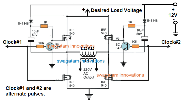
The working of the above H-bridge application design can be understood with the following points:
The crucial aspect here is to develop a voltage across the 10uF such that it becomes equal to the "desired load voltage" plus the supply 12V at the gates of the high side MOSFETs, during their ON periods.
The shown configuration executes this very efficiently.
Imagine clock#1 is high, and clock#2 is low (since they are supposed to be alternately clocking).
In this situation the top right mosfet becomes OFF, while the lower left mosfet is switched ON.
The 10uF capacitor quickly charges up to +12V through the 1N4148 diode and lower mosfet drain/source.
In the next instant, as soon as clock#1 becomes low and clock#2 becomes high, the charge across the left 10uF switches ON the top left MOSFET which immediately begins conducting.
In this situation its drain voltage begins rushing towards its source, and simultaneously the voltages starts pushing into the 10uF capacitor in such a way that the existing charge +12V "sits" over this instantaneously pushing voltages from the MOSFET terminal.
This addition of the drain potential into the 10uF capacitor through the source terminal ensures that the two potentials add up and enable the instantaneous potential across gate/source of the MOSFET to be just at around +12V above the drain potential.
For example if the drain voltage is selected to be 100V, then this 100V pushes into the 10uF causing a continuously compensating potential gate voltage which maintains at +12 just above the 100V.
I hope this helped you to understand the basic working of the high side bootstrapping using discrete capacitor diode network.
Conclusion
From the above discussion we understand that bootstrapping is crucial for all H-bridge topologies in order to allow effective switch ON of the high side mosfets.
In this process an appropriately selected capacitor across the gate/emitter of the High side mosfet is charged to 12V higher than the applied drain voltage level. Only when this happens the high side mosfets are able to switch ON and complete the intended push pull switching of the connected load.


Comments
Hi sir, am constructing inverter using ferrite core. I have successfully achieved 300v dc. But am having troubles converting the 300v dc to 220v ac. I need your help
Hi Chekwas, you will need a full bridge mosfet network with an oscillator circuit for transforming the 310V into 220V:
https://www.homemade-circuits.com/wp-content/uploads/2020/06/full-bridge-p-channel-1.jpg
Swagatam,
What if the desired voltage is 12v? Can one tie the desired voltage terminal to the 12+ and have the circuit still work?
Hi Cris, yes that’s definitely possible. You can use the last circuit as a 12 V full bridge circuit also.
Thanks! Can’t wait to try it
Hi,
Do you have any feedback diagrahm for the h-bridge circut using the 4047 ic
Hi, I don’t have it presently, but it can be easily configured
small mistake in your explanation…
“Imagine clock#1 is high, and clock#2 is low (since they are supposed to be alternately clocking).
In this situation the top right mosfet becomes OFF, while the lower left mosfet is switched ON.”
should be top LEFT should it not?
ie clock 1 turns lower left mosFET on, whilst turning on left hand BJT, which pulls upper left mosFET gate to ground, turning it off. clock 2 turns lower right mosFET off, along with right hand BJT, which then reverse biases right hand 1n4148 allowing right hand capacitor to apply 12v+source voltage to upper right hand mosFET gate.
Only the diagonally connected mosfets are supposed to remain switched ON at any instant of the oscillations, and the last circuit is fulfilling this requirement.
hello, very good tutorial, thankyou
I have a question! I use IR2110 for drive an H-bridge and my MOSFET is IRF1404.
When I turn on the circuit, In the unloaded state the output voltage is 12 volts, but when I connect the load the output voltage becomes zero! please help me to solve this problem. Thank you
Hello, Thanks for liking the post, after connecting the load check the frequency at the gate of the low side mosfets, if there’s no oscillations then your IC may not be working correctly…additionally make sure to connect a 1K across the gate source of each mosfet. Also make sure the SD pin is connected with the ground line….confirm whether the HIN, LIN inputs are correctly getting the oscillations from the external oscillators while the load is applied
Excellent tutorial. Thank a lot bro..
Thanks, it is my pleasure!
y como apago los mosfet altos para ponerlo a cargar las baterias?
Regarding this circuit, i think i got the main point of it, im trying to build a simple 3 phase vfd for a turbomolecular pump, and im stuck at this point this post has helped a lot, but i have one quick question:
Regarding the bc547 if i understodd correctly this transistor will be draining the cap to ground and this cap will be charged to the desired load voltage in my case above 100v plus the 12v for the gates, if this is the case, wouldnt we need to select an apropiate transistors for such voltages? or perhaps am i missing something.
Glad the post helped you to understand the concept.
Yes you are right, for 100V the transistor might need a change, although it may not be too crucial due to the presence of the 1k series resistor. But still for better safety you can use a 120 V rated transistor in your case….
Ok muy buena explicación ahora si entiendo gracias, el diodo no debe ser de recuperación rápida ?
Como calculo el condensador y la resistencia
The diodes can be fast recovery if the operating frequency is over 5 kHz, otherwise 1N4148 will do. The capacitor calculation is actually very complex, you can find the formula here:
https://www.homemade-circuits.com/arduino-3-phase-inverter-circuit-with-code/
Sir, i really glad to see this tutorial. I’ve been trying to understand why my h-bridge inverter high side mosfets getting warmer than low side mosfets.This topic really helped me.Thanks for sharing.
Thank you Muhammet, Glad it helped you!
Good day Swagatam, I want to appreciate you for your efforts. Please can you manufacturer pcb of some your projects? How much can it cost one for you to build pcb?
Thanks Offor, unfortunately presently I am not in the manufacturing business, so getting PCB may not be possible from me.
Good morning sir,
How will I add more mosfet to each to attain the wattage?
Like, I’m using irf44n which as 40A 55V
And what I want is 120A!
How Will I do the arrangement ?
Please I will love it if it been illustrated with a circuit diagram, thanks
Ajiboye,
you can add MOSFETs in parallel by joining their gate/drain/source together, just make sure the connections are as short as possible and adequately thick
Sir can I see a circuit diagram on how to do it sir
Hi 😉 I’ve simulated the circuit above in LTSpice. I get extreme current spikes on the supply voltage (short circuits) due to the upper and lower mosfets both conducting at the same time during clock level transitions. Separating the clock line and providing dedicated clocks with some deadtime inbetween solves the problem. I wonder how you got around that problem in your practical implementations?
Good afternoon sir, I’m having a serious challenge, I build a hbridge and I build the boostrapimg drive the hbrigd while sg3524 is use to drive the boostrap for but when ever I power it my mosfet blown or at times the voltage will drop to the extent that ther will be no output from the oscillator board, but if I power the oscillator board alone it works fine. Please what could be the cause
Hi Faith, which circuit did you build? Please show me the schematic…
Thanks swagatam for such an informative blog. I really appreciate it.
Thank you Rick! Glad you liked it!