As the name suggests, an inverter circuit that converts a DC input into AC without depending on an inductor or a transformer is called a transformerless inverter.
Since an inductor based transformer is not employed, the input DC is normally equal to the peak value of the AC generated at the output of the inverter.
The post helps us to understand 3 inverter circuits designed to work without using a transformer, and using a full bridge IC network and a SPWM generator circuit.
Transformerless Inverter using IC 4047
Let's begin with an H-Bridge topology that's probably the simplest in its form. However, technically it's not the ideal one, and not recommended, since It is designed using p/n-channel mosfets. P-channel mosfets are used as the high side mosfets, and n-channel as the low side.
Since, p-channel mosfets are used on the high side, the bootstrapping becomes unnecessary, and this simplifies the design a lot. This also means this design does not have to depend on special driver ICs.
Although the design looks cool and enticing, it has a few underlying disadvantages. And that's exactly why this topology is avoided in professional and commercial units.
That said, if it's built correctly may serve the purpose for low frequency applications.
Here's the complete circuit using IC 4047 as the astable totem pole frequency generator
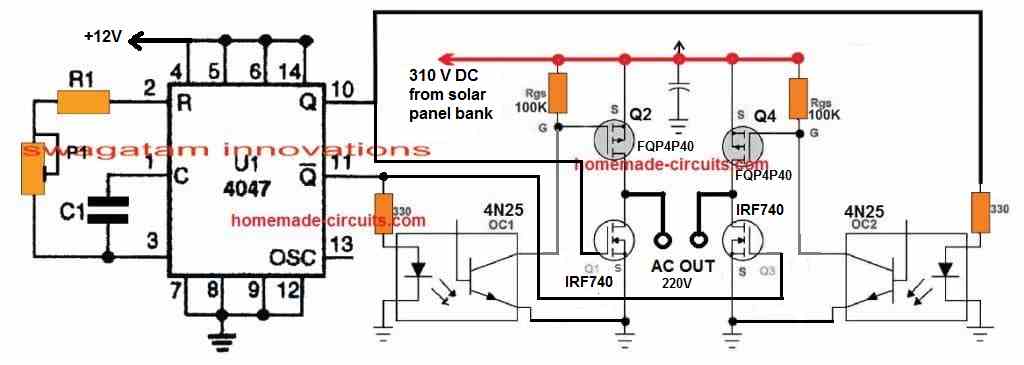
Parts List
All resistors are 1/4 watt 5%
- R1 = 56k
- C1 = 0.1uF / PPC
- IC pin10/11 resistor = 330 ohms - 2nos
- MOSFET gate resistors = 100k - 2nos
- Opto-couplers = 4N25 - 2 nos
- Upper P-channel MOSFETs = FQP4P40 - 2nos
- Lower N-Channel MOSFETs = IRF740 = 2nos
- Zener diodes = 12V, 1/2 watt - 2 nos
The next idea is also an h-bridge circuit but this one uses the recommended n-channel mosfets. The circuit was requested by Mr. Ralph Wiechert
Main Specifications
Greetings from Saint Louis, Missouri.
Would you be willing to collaborate on an inverter project? I would pay you for a design and/or your time, if you'd like.
I have a 2012 & 2013 Prius, and my mother has a 2007 Prius. The Prius is unique in that it has a 200 VDC (nominal) high-voltage battery pack. Prius owners in the past have tapped into this battery pack with off-the-shelf inverters to output their native voltages and run tools and appliances. (Here in the USA, 60 Hz, 120 & 240 VAC, as I'm sure you know). The problem is those inverters are no-longer made, but the Prius is still is.
Here are a couple inverters that were used in the past for this purpose:
1) PWRI2000S240VDC (See attachment) No longer manufactured!
2)Emerson Liebert Upstation S (This is actually a UPS, but you remove the battery pack, which was 192 VDC nominal.) (See attachment.) No longer manufactured!
Ideally, I'm looking to design a 3000 Watt continuous inverter, pure sine wave, output 60 Hz, 120 VAC (with 240 VAC split phase, if possible), and transformer-less. Perhaps 4000-5000 Watts peak. Input: 180-240 VDC. Quite a wish-list, I know.
I am a mechanical engineer, with some experience building circuits, as well as programming Picaxe micro-controllers. I just don't have much experience designing circuits from scratch. I'm willing to try & to fail, if needed!
The Design
In this blog I have already discussed more than 100 inverter designs and concepts, the above request can be easily accomplished by modifying one of my existing designs, and tried for the given application.
For any transformerless design there has to be a couple of basic things included for the implementation: 1) The inverter must be a full bridge inverter using a full bridge driver and 2) the fed input DC supply must be equal to the required output peak voltage level.
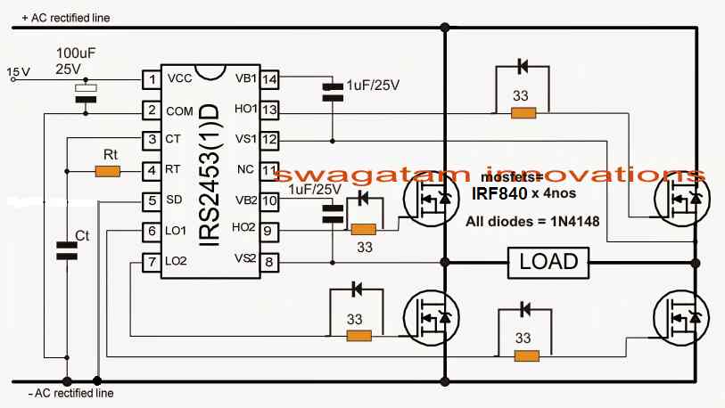
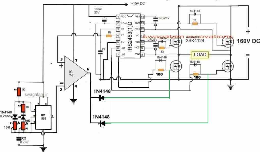
Incorporating the above two factors, a basic 3000 watt inverter design can be witnessed in the following diagram, which has a pure sinewave output waveform feature.
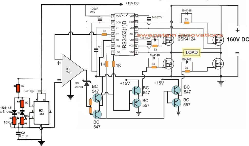
The above diagram can be further simplified as shown in the following figures:
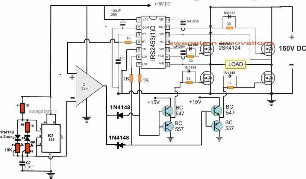
The functioning details of the inverter can be understood with the help of the following points:
The basic or the standard full bridge inverter configuration is formed by the full bridge driver IC IRS2453 and the associated mosfet network.
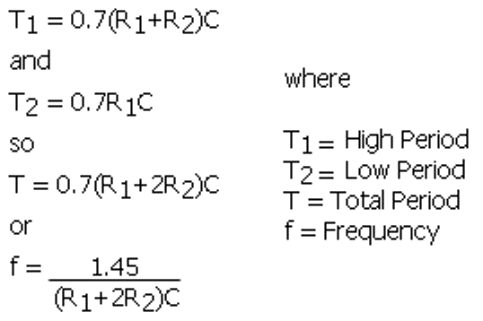
Calculating the Inverter Frequency
The function of this stage is to oscillate the connected load between the mosfets at a given frequency rate as determined by the values of the Rt/Ct network.
The values of these timing RC components can be set by the formula: f = 1/1.453 x Rt x Ct where Rt is in Ohms and Ct in Farads. It should be set for achieving 60Hz for complementing the specified 120V output, alternatively for 220V specs this could be changed to 50Hz.
This may be also achieved through some practical trial and error, by assessing the frequency range with a digital frequency meter.
For achieving a pure sinewave outcome, the low-side mosfets gates are disconnected from their respective IC feeds, and are applied the same through a BJT buffer stage, configured to operate through an SPWM input.
Generating SPWM
The SPWM which stands for sinewave pulse width modulation is configured around an opamp IC and a single IC 555 PWM geneartor.
Although the IC 555 are configured as PWM, the PWM output from its pin#3 is never used, rather the triangle waves generated across its timing capacitor is utilized for the carving of the SPWMs.
Here one of the triangle wave samples is supposed to be much slower in frequency, and synchronized with the main IC's frequency, while the other needs to be faster triangle waves, whose frequency essentially determines the number of pillars the SPWM may have.
The opamp is configured like a comparator and is fed with triangle wave samples for processing out the required SPWMs. One triangle wave which is the slower one is extracted from the Ct pinout of the main IC IRS2453
The processing is done by the opamp IC by comparing the two triangle waves at its input pinouts, and the generated SPWM is applied to the bases of the BJT buffer stage.
The BJTs buffers switch according to the SPWM pulses and make sure that the low side mosfets are also switched at the same pattern.
The above switching enables the output AC also to switch with an SPWM pattern for both the cycles of the AC frequecny waveform.
Selecting the mosfets
Since a 3kva transformerless inverter is specified, the mosfets need to be rated appropriately for handling this load.
The mosfet number 2SK 4124 indicated in the diagram will actually not be able to sustain a 3kva load because these are rated to handle a maximum of 2kva.
Some research on the net allows us to find the mosfet: IRFB4137PBF-ND which looks good for operating over 3kva loads, due to its massive power rating at 300V/38amps.
Since it is a transformerless 3kva inverter, the question of selecting transformer is eliminated, however the batteries must be appropriately rated to produce a minimum of 160V while moderately charged, and around 190V when fully charged.
Automatic Voltage Correction.
An automatic correction can be achieved by hooking up a feedback network between the output terminals and the Ct pinout, but this may be actually not required because the IC 555 pots can be effectively used for fixing the RMS of the output voltage, and once set the output voltage can be expected to be absolutely fixed and constant regardless of the load conditions, but only as long as the load does not exceed the maximum power capacity of the inverter.
2) Transformerless Inverter with Battery Charger and Feedback Control
The second circuit diagram of a compact transformeress inverter without incorporating bulky iron transformer is discussed below. Instead of an heavy iron transformer it uses a ferrite core inductor as shown in the following article.
The schematic is not designed by me, it was provided to me by one of the avid readers of this blog Mr. Ritesh.
The design is a full fledged configuration with includes most of the features such as ferrite transformer winding details, low voltage indicator stage, output voltage regulation facility etc.
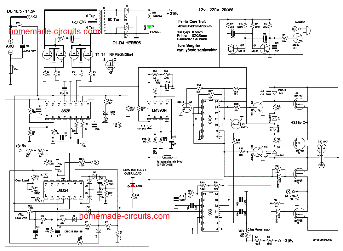
The explanation for the above design hasn't been updated yet, I will try to update it soon, in the meantime you can refer the diagram and get your doubts clarified through comment, if any.
200 watt Compact Transformerless Inverter Design#3
A third design below shows a 200 watt inverter circuit without a transformer (transformerless) using a 310V DC input. It is a sine wave compatible design.
Introduction
Inverters as we know are devices which convert or rather invert a low voltage DC source to a high voltage AC output.
The produced high voltage AC output is generally in the order of the local mains voltage levels. However the conversion process from a low voltage to high voltage invariably necessitates the inclusion of hefty and bulky transformers. Do we have an option to avoid these and make a transformerless inverter circuit?
Yes there is a rather very simple way of implementing a transformerless inverter design.
Basically inverter utilizing low DC voltage battery require to boost them to the intended higher AC voltage which in turn makes the inclusion of a transformer imperative.
That means if we could just replace the input low voltage DC with a DC level equal to the intended output AC level, the need of a transformer could be simply eliminated.
The circuit diagram incorporates a high voltage DC input for operating a simple mosfet inverter circuit and we can clearly see that there's no transformer involved.
Circuit Operation
The high voltage DC equal to the required output AC derived by arranging 18 small, 12 volt batteries in series.
The gate N1 is from the IC 4093, N1 has been configured as the oscillator here.
Since the IC requires a strict operating voltage between 5 and 15 volts,the required input is taken from one of the 12 volt batteries and applied to the relevant IC pin outs.
The entire configuration thus becomes very simple and efficient and completely eliminates the need of a bulky and heavy transformer.
The batteries are all 12 volt, 4 AH rated which are quite small and even when connected together does not seem to cover too much of space.They may stacked tightly to form a compact unit.
The output will be 110 V AC at 200 watts.
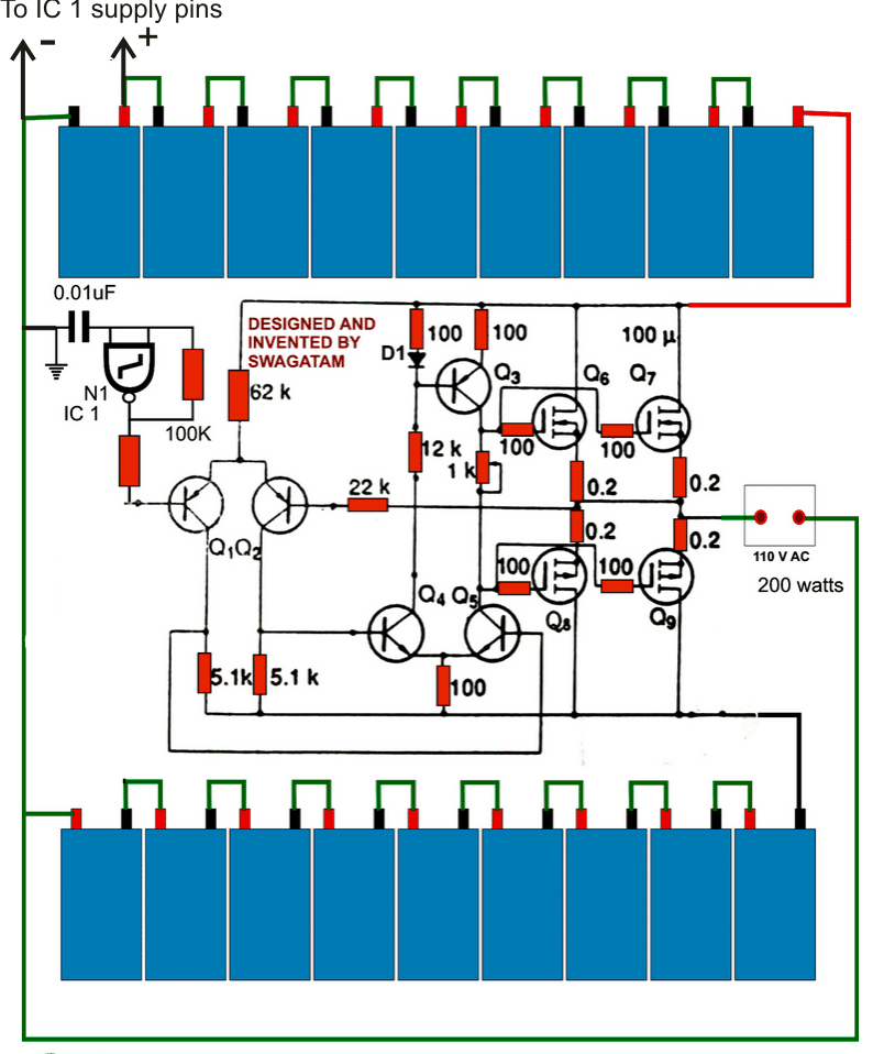
Parts List
- Q1, Q2 = MPSA92
- Q3 = MJE350
- Q4, Q5 = MJE340
- Q6, Q7 = K1058,
- Q8, Q9 = J162
- NAND IC = 4093,
- D1 = 1N4148
- Battery = 12V/4AH, 18 nos.
Upgrading into a Sinewave Version
The above discussed simple 220V transformerless inverter circuit could be upgraded into a pure or true sinewave inverter simply by replacing the input oscillator with a sine wave generator circuit as shown below:
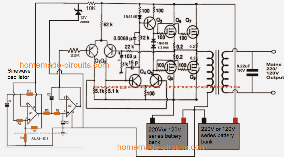
Parts List for the sinewave oscillator can be found in this post
Transformerless Solar Inverter Circuit
Sun is a major and an unlimited source of raw power which is available on our planet absolutely free. This power is fundamentally in the form of heat, however humans have discovered methods of exploiting the light also from this huge source for manufacturing electrical power.
Overview
Today electricity has become the life line of all cities and even the rural areas. With depleting fossil fuel, sun light promises to be one of the major renewable source of energy that can be accessed directly from anywhere and under all circumstances on this planet, free of cost. I have explained one of the methods of converting solar energy into electricity for our personal benefits.
In one of my previous posts I have discussed a solar inverter circuit which rather had a simple approach and incorporated an ordinary inverter topology using a transformer.
Transformers as we all know are bulky, heavy and may become quite inconvenient for some applications.
In the present design I have tried to eliminate the use of a transformer by incorporating high voltage mosfets and by stepping up the voltage through series connection of solar panels. Let's study the whole configuration the with the help of the following points:
How it Works
Looking at the below shown solar based transformerless inverter circuit diagram, we can see that it basically consists of three main stages, viz. the oscillator stage made up of the versatile IC 555, the output stage consisting of a couple of high voltage power mosfets and the power delivering stage which employs the solar panel bank, which is fed at B1 and B2.
Circuit Diagram
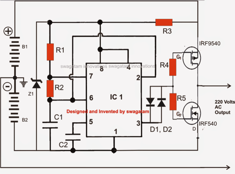
Since the IC cannot operate with at voltages more than 15V, it is well guarded through a dropping resistor and a zener diode. The zener diode limits the high voltage from the solar panel at the connected 15V zener voltage.
However the mosfets are allowed to be operated with the full solar output voltage, which may lie anywhere between 200 to 260 volts. On overcast conditions the voltage might drop to well below 170V, So probably a voltage stabilizer may be used at the output for regulating the output voltage under such situations.
The mosfets are N and P types which form a pair for implementing the push pull actions and for generating the required AC.
The mosfets arenot specified in the diagram, ideally they must be rated at 450V and 5 amps, you will come across many variants, if you google a bit over the net.
The used solar panels should strictly have an open circuit voltage of around 24V at full sunlight and around 17V during bright dusk periods.
How to Connect the Solar Panels
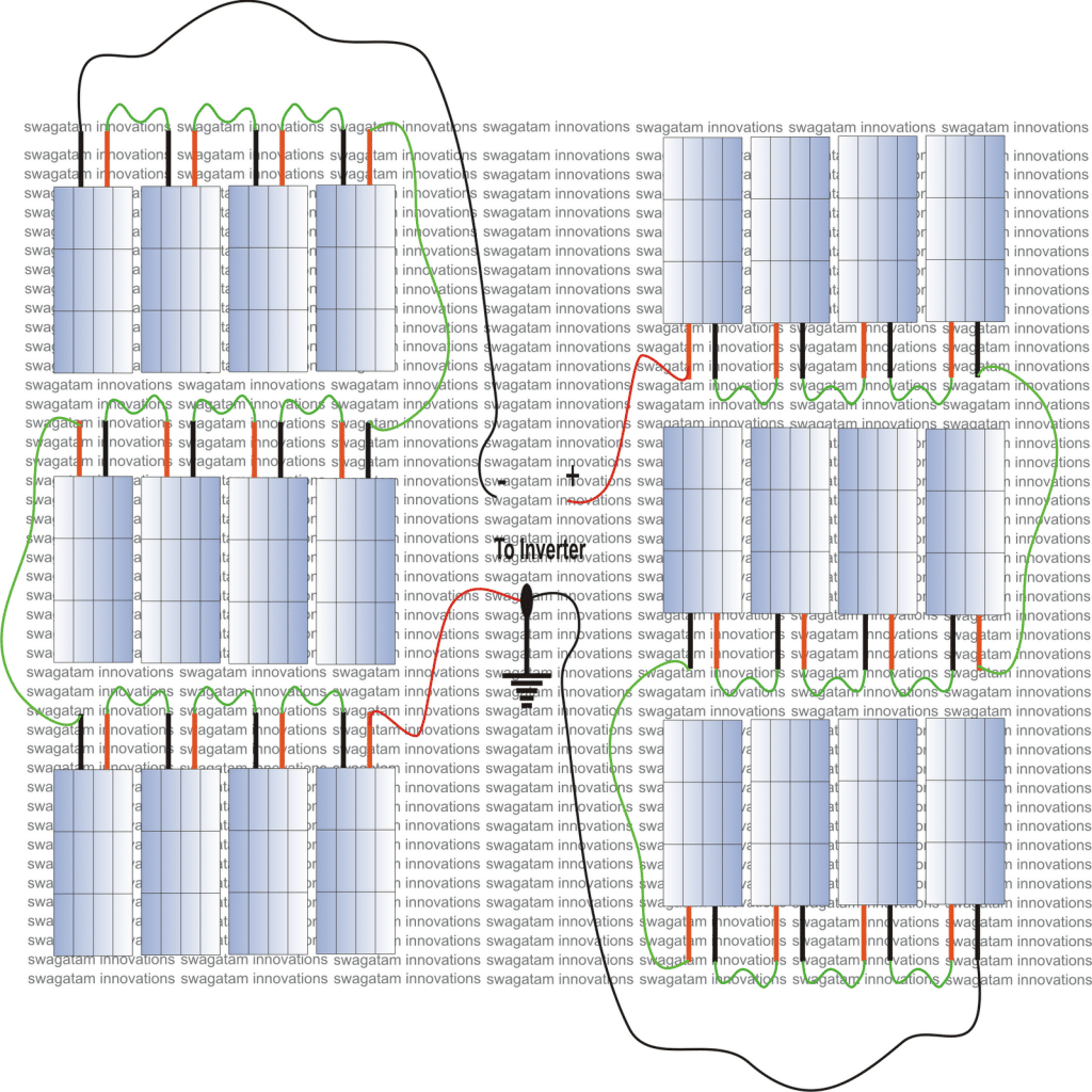
Parts List
R1 = 6K8
R2 = 140K
C1 = 0.1uF
Diodes = are 1N4148
R3 = 10K, 10 watts,
R4, R5 = 100 Ohms, 1/4 watt
B1 and B2 = from solar panel
Z1 = 5.1V 1 watt
Use these formulas for calculating R1, R2, C1....
Update:
The above 555 IC design may not be so reliable and efficient, a much reliable design can be seen below in the form of a full H-bridge inverter circuit. This design can be expected of providing much better results than the above 555 IC circuit.
Another advantage of using the above circuit is that you won't require a dual solar panel arrangement, rather a single series connected solar supply would be enough to operate the above circuit for achieving a 220V output.


Comments (272)
These transformerless inverter circuit components can they be found for purchase and work perfectly ?
I would recommend the following design:

If implemented step-wise, with proper understanding, it will work as intended.
Hello
Do you know if there is a circuit schematic I can get that would show me how to build a 20 kw 220 vac split phase inverter 48-volt dc supply
Hi,
I don’t have this circuit with me right now, but it is not difficult to design one. I will do it soon and post it in this blog as a new article.
Dear Sir,
Can I use Fairchild 41N60E?
Rds 41mohms
VDs600
ID77
Input capacitance 13000pf
Qg385nc
Yes, you can use it.
Hi Sir,
As I apply 175v AC which after filter became 175*1.4=245vdc, I have applied 1u 400 volt polyester capacitor between the highside source pin that means between the load. I also uses irfp264n mosfets which is 250 vDC with 44amp rated.
When I apply power the 1u capacitor became leaked and a liquid substance drowning from its body and the line MCB cutoff when I forcefully on the MCB then a blast occurred at the MOSFET high side drain pin with black charge spot on the pcb, all the MOSFET are dead.
I also observed when I apply 25vdc power at the MOSFET then the output gives 25v AC but when I Apply 110volt DC then the output voltage fluctuates as 47, 97,109 vac and when 245vdc given the output became 570,289,330 as well as input also fluctuates.
Hi Rinku,
If your supply voltage is 250V then the MOSFETs must be rated at least 300V or ideally 500V.
https://www.vishay.com/docs/91070/91070.pdf
Your 1uF capacitor could be faulty or not rated to handle 250V. Try a good quality PPC 105/400V capacitor.
If you supply 250V to the H-bridge, the output will also be 250V, it cannot fluctuate between 570V or 289V. If this happening, it is due to your meter instability, and due to high inverter frequency.
Make sure the inverter frequency is 50Hz.
Always connect a fuse in series with the supply.
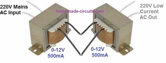
For initial testing you can use a low current AC supply through transformer connected in the following manner.
Good morning Sir.
Thanks for the above schematics.
I wish to ask for a good schematic if an inverter that can be powered by high voltage (100VDC – 450VDC) from solar panels even without battery.
And can also charge a battery for a 24V or 48V solar system
Good morning Ngang,
you can use the H-bridge designs explained in the above article for making your 450V inverter project.
For charging the battery you can try the last circuit from the following article:
https://www.homemade-circuits.com/make-this-48v-automatic-battery-charger/
Good morning Sir,
As per above link I have added three transformer to achieve 100 volt AC which after filter became 138vdc and 100 watt bulb filament glowing red as we observe when our domestic line became single phase.
My spwm signal output at 4500Hz
Output load frequency is at 50.03Hz with sinewave pulse.
The output frequency have measured when I gave 25volt supply. I have not tested it with 220 vac or 110 vdc..
But I have measured direct 220 AC wave form which is similar to that of 25 volt wave form I supplied to mosfets.
Rinku, since the transformer current is low, you can try a 25 watt or a 10 watt bulb as the load.
Rest everything looks OK to me at the moment.
Good morning Sir,
Have question regarding testing the full bridge inverter.
As I have no solar panel at this moment I tried connecting a stabilizer 175volt tapping with a 35 amp bridge rectifier supplying 210vdc, the output is connected 100watt 230volt bulb when I apply AC current the bulb glows fully but the stabilizer fuse immediately blown up.
The 12 volt is supplied through a 12 volt adaptor separately though no inverter parts are damaged yet
Hello Rinku,
Try with a 40 watt bulb, and check whether the fuse blows or not. I think the fuse is not rated to handle 100 watts.
Hi Sir,
But the stabilizer is serving my refrigerator which is operated by 120 watt compressor
If there was a short circuit in the h-bridge, the bulb would never glow, but since the 100 watt bub is glowing that means the h-bridge is working ok.
Still i would recommend checking with a 40 watt bulb, if there’s a short circuit the fuse would blow again.
Hi Sir,
I connected the 1000ufd 400 volt capacitor to DC line and the fuse blown immediately but when I remove the positive connection then it ok.
Hi Rinku, When you switch ON power the 1000uF acts like a momentary short circuit, until it charges fully, this momentary short circuit could be causing the fuse to blow. Try a 10 ohm or 20 ohm resistor in series with the 1000uF and check.
Or use an NTC thermistor in series with the supply, that might help.
Dear sir,
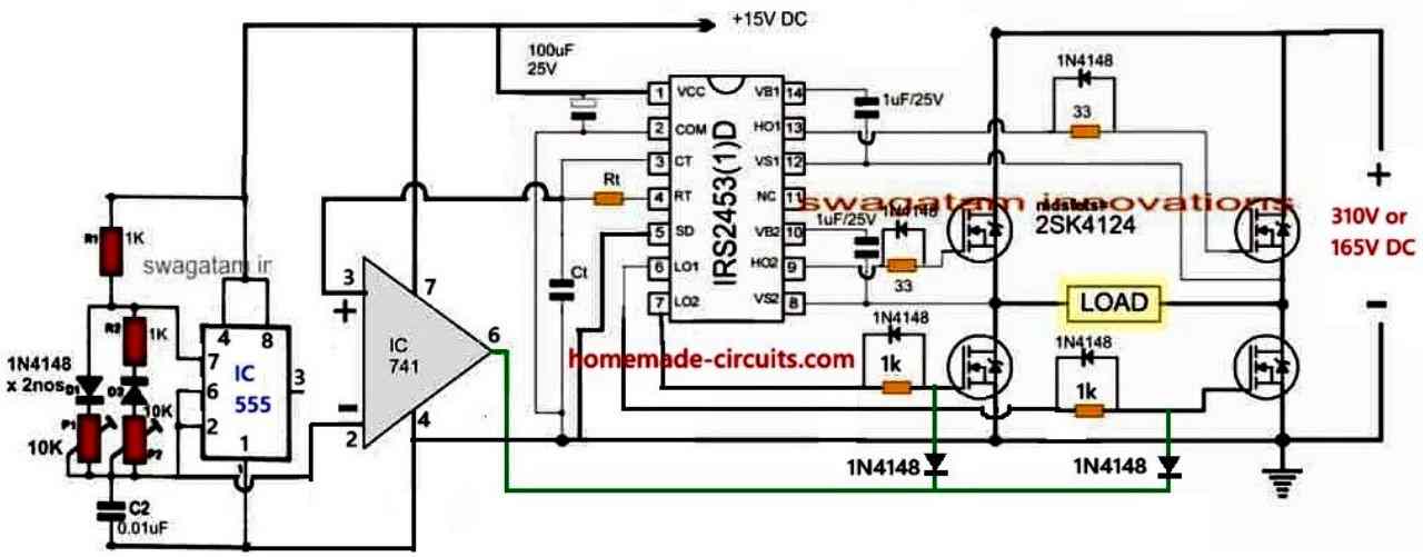
Please elaborate this issue and enlighten me what happens here when punching SPWM signal to lowside mosfets,why should we use reverse diode? If I use 1 k resistor between pin 6&7 (2453ic) and gates and connect the spwm with two forward diode directly to gates the gate voltage is 7.8 and 8.1 volt respectively
The spwm & triangle generated by lm 324 is great and spwm output is 3.45volt
Hi Rinku,
You can use 1k resistor as the gate resistors for the low side MOSFETs but do not forget to add the parallel diodes across these 1k resistors, otherwise the low side MOSFETs might heat up.
The idea is to chop each 50 Hz square wave pulse at the low side MOSFFET gates into pieces replicating the SPWM waveform. So we want to create the notches or the OFF periods on these 50 Hz pulse which are exactly similar to the SPWM pulse notches.
Notches are the gaps that are present in our SPWM cycles.
During these notch periods or the OFF periods of the SPWM, the 50 Hz cycles are pulled to ground through the reverse 1N4148 diodes, into the 741 IC pin6 creating a similar off period on the 50 Hz cycles, at the MOOSFET gate.
So whenever we have the off periods in the SPWM, the 50Hz pulse on the gate are pulled to ground through the diodes and the 741 pin#6 which causes identical off periods to be carved in those 50 Hz gate pulses.
To enable the off periods to react on the 50Hz pulses we need reverse diodes only, the forward diodes would block these off periods so we cannot use forwards diodes.
Dear Sir,
Please tell me which one is correct or both are wrong
https://quickshare.samsungcloud.com/aBaFstfHFyhc
Hi Rinku, both are wrong, the SPWM can be replicated at the low side gates only with negative pulses, and that is why the diodes needs to be reverse biased and not forward biased. If you use forward biased diodes it will have no effect on the MOSFET gates.
I have explained you in the earlier comment regarding how the diodes work.
Hello Sir,
So final result is, if the spwm reverse diode connection is open then the signal can be measured with respect to +12 volt and if reverse diode connected directly with gates then no signal can be measured with respect to positive or negative only 50 Hz pulse will reflect.
Yes, If the spwm is connected with the gates through reverse diodes, then you can measure the gate waveform by attaching the scope probes across the gate/source of the mosfets.
Dear Sir,
Below is the comparison of ct pin 3 of 2453ic and spwm at 741 output
https://quickshare.samsungcloud.com/csKiCFtxcNSZ
This diagram is much better and clearly shows the spwm in response to the slow triangle waves from the CT pin of the inverter IC. The spwm output from ic 741 is confirmed now.
Good afternoon Sir,
Below is the spwm out from 741 with respect to ground
https://quickshare.samsungcloud.com/jlEj0Ur97PLa
Hello Rinku, the full spwm cycle is not visible in this image, so I cannot confirm it.
Dear Sir,
Apologi to disturb you again
The channel 2 showing spwm output of 741 and channel 1 showing high side source between/load frequency
https://quickshare.samsungcloud.com/fQoZBQAKFj8Z
Diode have removed from 741 output added 1 k resistor to base of bjt buffer with 220R ground
Hello Rinku, The SPWM is not clear, that is why had I told you to first confirm the SPWM from IC741 before integrating with the low side MOSFETs.
Please disconnect the pin#6 of 741 from the inverter circuit.
Check the SPWM between pin#6 of 741 and ground. For each triangle wave pulse from the CT pin of IRS2453 there should one set of SPWM generated at pin#6 of IC 741.
Only after confirming the above, integrate the 741 output with the low side MOSFETs in the following manner:
Remember to change the low side gate resistor to 100 ohms and USE REVERSE 1N4148 DIODES PARALLEL TO THE GATE RESISTORS, as shown in the diagram.
Good morning Sir,
Below is the pin6 wave form of ic 741
https://quickshare.samsungcloud.com/eF9DLcvxOTEB
This waveform is valid only at the cathode of diode when the MOSFET vds voltage is applied and if the supply voltage is discontinued then it reflect to gate of lowsides mosfets while the 12 volt is supplied to ic 741,555&2453
So what is the reason when MOSFET vdd given frequency disappear from gate and while supply disconnect and bulb is off then the spwm signal appears.
What’s the reason?
I am frustrated
Hi Rinku,
I can only help you to understand the circuit and implement it, I cannot troubleshoot your circuit because I cannot practically check it. If I could check your circuit I could quickly solve it for you.
Please understand the working of the SPWM and if you have understood it, implement it accordingly.
The positive peaks of the SPWM will have no effect on the totem pole base and therefore have no effect on the gate of the low side MOSFETs,
However, the negatives of the SPWM which are in the form of valleys or gaps, will turn OFF the BC547 BJT and the gate voltage of the low side MOSFET, in this way it will chop the low side MOSFET gate and force the H-Bridge to oscillate with the SPWM pattern. This will create the intended sine wave output on the load.
Are you building this circuit on breadboard? If yes then please build it on a strip board by soldering.
Your SPWM image looks somewhat OK, but I cannot see the full start to end of the waveform, please make the range smaller and try to get at least two consecutive cycles of the SPWM.
Good morning Sir,
As per your instructions I have measured the frequency and it is bunch of 5 bars but the output I measured connected both probe at source of each highside mosfets it shows neat and clean 50 Hz with 50% duty cycle frequency and if I detach one probe with remaining at one probe at source and the other with output of 741 then it shows nice sinewave picture, I just touch the output and detach it and this is the result.
Please guide me
The bulb glow at full with 21 volt AC
This voltage cannot measure in the DC range of my multimeter
Regards
Good Morning Rinku,
Please confirm the spwm waveform across the pin#6 of ic 741 and ground, across gate/source of the low side MOSFETs. Finally, confirm the above between the sources of the upper two high side mosfets. If your oscilloscope shows the spwm waveform correctly across the above sections that would confirm the sine wave working of the inverter. Remember, to get a pure sinewave you will need a transformer across the h-bridge output.
Hi Engineer Sir,
Can I operate this load terminal directly with any electrical machines or it will require a transformer such as voltage stabilizer transformer through which I can run motor, fans etc, as this is a transformer less inverter will it requires a stepup transformer or you recommend a stepdown transformer to measure the frequency only whether it produce sinewave or not.
Hi Rinku,
You can connect a load directly across the load terminals, no need of a transformer. But if you use 12V DC as the supply and use a 12V to 220V transformer across the load terminals then that will help you to generate a pure sine wave 220V output.
Dear Sir,
It means if I use solar 160vdc as input I cannot make it pure sine wave then how to get pure sinewave if I use solar series power as my input, in that case which transformer I can use to convert it sinewave? If I use transformer the efficiency of inverter will be hampered,it will give only 65%
Hi Rinku, you can get a pure sinewave even without a transformer. How much pure the sinewave can be depends upon how many pillars you use inside each spwm waveform. You can increase the frequency of the fast triangle waves in order to increase the number of pillars inside each spwm….The more numbers you have the better will be the purity of the sine waveform.
Yes Engineer that’s the solution I want to hear from you as you wrote in this edition about 330Hz frequency limitation I can’t go to test for higher frequency because if it blown the mosfets. If I apply 1kHz spwm signal then the ratio would be 1:20 , will the mosfets remain live?
Another question please clarify::
The pin 6&7 of 2453 ic giving 6 volt mean and pk to 12 volt when I add diode to output of 741 ic the voltage became half why this happens?
MOSFETs can handle frequencies in GHz, so increasing frequency in kHz will not blow a MOSFET, unless there’s some other reasons.
330Hz is recommended if an iron core transformer is used at the output, otherwise not.
Yes, the SPWM will reduce the conduction rate by around 50%, that is why your seeing 50% drop in the pin6/7 voltages, but the peak will be 12V
Hi Sir,
Good evening, the diode you have used in your modified transformerless inverter 741opamp output to pass signal to totempoll base is not giving any spwm signal as voltage cannot passes through cathode of diode similarly signal also blocked by the diode 4148,so what should we do to carry the signal,if we direct the output to base of totem it will damage the mosfets as well the 2453 ic as high current pass through.
I have connected 10 k resistor from 741output to bjt base with grounding it by 1 k resistor and the low side gate voltage (mean) is 3.7v .but as I supply power to mosfet the magnitude of signal decreases.
Please solve this problem
Hi Rinku, the output from the diode is supposed to be negative, not positive, so you can check the SPWM across the diode output and the positive line.
First of all is your basic inverter working without the 741 SPWM, remember I told you to confirm that first?
Also, are you using an oscilloscope to confirm the SPWM. Without an oscilloscope it is impossible to check and troubleshoot this inverter circuit.
If you don’t have an oscilloscope you can buy the following one:
https://www.homemade-circuits.com/dso138-best-small-oscilloscope-for-electronic-hobbyists/
Hi Sir,
The primary circuit is working fine without the 741,there is no voltage drop at the load output.
I am measuring the diode frequency with respect to ground as the voltage is negative as you are saying, so where my scope will display the frequency?
So I have to measure it with respect to positive voltage
One probe should be connected with anode of diode and the other with +VCC.
Yes, that’s right, you have to check the 741 output in that manner….but the waveform is most important, you must confirm whether you are getting the exact spwm waveform or not.
Good evening Sir,
Please tell me about parameters of SPWM wave i.e. the time division and voltage division and duty cycle so that I can match it with my scope.
Thanks for your support
Goodnight
Rinku
Hello Rinku, the SPWM should look like this:
Yes Sir,
How many tricks have to learn from you to discover this transformerless inverter, God knows
Hi Engineer,
I am facing problem with HO2 MOSFET which blown twice with casualty of 2453 ics HO1 voltage absence and pin14 capacitor not charging but remaining part of ic is ok,, This happened because I modify the totem driver with 3.3 volt zener with 10k resistor as the diode (your modified circuit) connected to totem doesn’t carry the spwm signal(very low) to the lowside. Now the 741 out signal is 330Hz and totempoll output is 268 HZ,How should I protect the ic from reverse current? Should I change the highside diode direction from reverse to forward and apply a gate source NPN transistor to catch the reverse current, but here is one major drawback that the gate voltage never became zero.
Plz give your valuable comment.
শুভ রাত্রি
রিঙ্কু
Hi Rinku,
You must build the inverter in a step by step manner.
First build the basic square wave inverter without the IC 741 and the IC555 and without the totem pole transistor stage. Connect the LO1 and LO2 directly to the low side mosfet gates though the 33 ohms resistors.
If you succeed, then try adding the low side totem pole transistors. If everything goes fine, after that you can try configuring the IC 741 and the IC 555 stages correctly by verifying the various waveform through an oscilloscope and meters.
There are no 3.3V zeners in the design so you must not use them anywhere.
Thank you Rinku, for posting your question.
The low side MOSFETs will be driven by the 330 Hz frequency, since each set of the SPWM cycle which is equivalent to one sinewave cycle will have 330Hz frequency.
The best place to check the IR2453 frequency across its Ct pin and across the low side outputs.