In this article I have explained the pinout functions of the IC SG3525 which is a regulating pulse width modulator IC. So I have explained in details:
Main Technical Features
The main features of the IC SG3525 may be understood with the following points:
- Operating voltage = 8 to 35V
- Error amp reference voltage internally regulated to 5.1V
- Oscillator frequency is variable through an external resistor within the range of 100Hz to 500 kHz.
- Facilitates a separate oscillator sync pinout.
- Dead time control is also variable as per intended specs.
- Has an internal soft start feature
- Shut down facility features a pulse by pulse shutdown enhancement.
- Input under voltage shut down feature also is included.
- PWM pulses are controlled through latching for inhibiting multiple pulse outputs or generation.
- Output supports a dual totem pole driver configuration.
Pinout Diagram of the IC
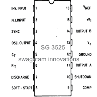
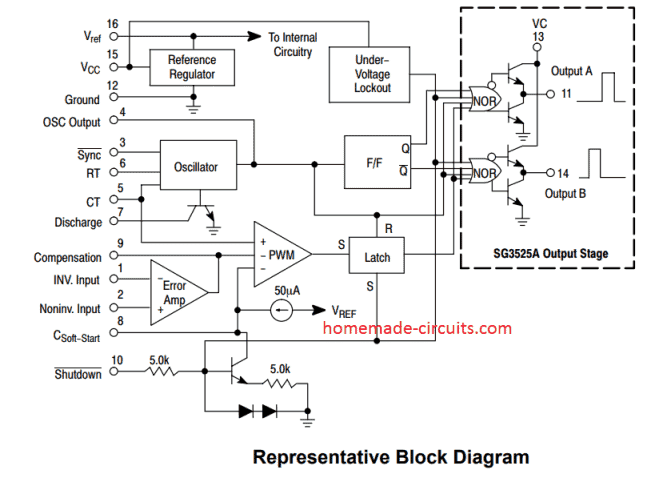
SG3525 PinOut Description
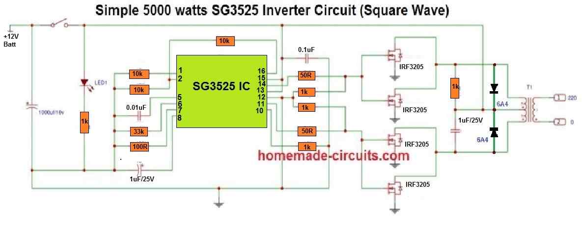
A practical implementation of the following pinout data may be understood through this inverter circuit
The IC SG3525 is a single package multi function PWM generator IC, the main operations of the respective pin outs are explained with the following points:
Pin#1 and #2 (EA inputs): These are inputs of the built-in error amplifier of the IC. Pin#1 is the inverting input while pin#2 is the complementary non-inverting input.
It's a simple op amp arrangement inside the IC which controls the PWM of the IC outputs at Pin#11 and Pin#14. Thus these EA pins 1 and 2 can be effectively configured for implementing an automatic the output voltage correction of a converter.
It is usually done by applying a feedback voltage from the output through a voltage divider network to the non-inverting input of the op amp (pin#1).
The feedback voltage should be adjusted to be just below the internal reference voltage value (5.1 V) when the output is normal.
Now, if the output voltage tends to increase above this set limit, the feedback voltage would also increase proportionately and at some point exceed the reference limit. This will prompt the IC to take necessary corrective measures by adjusting the output PWM, so that the voltage is restricted to the normal level.
Pin#3 (Sync): This pinout can be used for synchronizing the IC with an external oscillator frequency. This is generally done when more than a single IC is used and requires to be controlled with a common oscillator frequency.
Pin#4 (Osc. Out): It's the oscillator output of the IC, the frequency of the IC may be confirmed at this pin out.
Pin#5 and #6 (Ct, Rt): These are termed CT, RT respectively. Basically these pinouts are connected with an external resistor and a capacitor for setting up the frequency of the inbuilt oscillator stage or circuit. Ct must be attached with a calculated capacitor while the Rt pin with a resistor for optimizing the frequency of the IC.
The formula for calculating the frequency of IC SG3525 with respect to RT and CT is given below:
f = 1 / Ct(0.7RT + 3RD)
- Where, f = Frequency (in Hertz)
- CT = Timing Capacitor at pin#5 (in Farads)
- RT = Timing Resistor at pin#6 (in Ohms)
- RD = Deadtime resistor connected between pin#5 and pin#7 (in Ohms)
Pin#7 (discharge): This pinout can be used for determining the deadtime of the IC, meaning the time gap between the switching of the two outputs of the IC (A and B). A resistor connected across this pin#7 and pin#5 fixes the dead time of the IC.
Pin#8 (Soft Start): This pinout as the name suggests is used for initiating the operations of the IC softly instead of a sudden or an abrupt start. The capacitor connected across this pin and ground decides the level of soft initialization of the output of the IC.
Pin#9 (Compensation): This pinout is for compensating the error amplifier op amp. Mostly this pinout is connected to ground via a RC network. However, if required this pinout can be configured with an external transistor which can ground this pin during a critical situation, enabling a shutdown of the IC output.
Why Compensation Network is Required at pin#9
See, if you connect feedback directly without compensation then things do not stay calm, they start misbehaving.
The system can oscillate, like it keeps shaking instead of settling. Output voltage can go up and down.
If load changes then it may become unstable, especially under sudden load change and then you may see strange behavior.
We therefore do not leave it just open..
So we connect a resistor. We also connect a capacitor. Sometimes an RC network between Pin#9 and ground, but sometimes also to feedback pin, depends on how it is arranged.
This then forms what we call a compensation network for the SG3525 IC.
Pin#10 (Shutdown): As the name suggest this pinout may be used for shutting down the outputs of the IC in an event of a circuit malfunction or some drastic conditions.
A logic high at this pin out will instantly narrow down the PWM pulses to the maximum possible level making the output device's current go down to minimal levels.
However if the logic high persists for longer period of time, the IC prompts the slow start capacitor to discharge, initiating a slow turn ON and release. This pinout should not be kept unconnected for avoiding stray signal pick ups.
Pin#11 and #14 (output A and output B): These are the two outputs of the IC which operate in a totem pole configuration or simply in a flip flop or push pull manner.
External devices which are intended for controlling the converter transformers are integrated with these pinouts for implementing the final operations.
Pin#12 (ground): It's the ground pin of the IV or the Vss.
Pin#13 (Vcc): The output to A and B are switched via the supply applied to pin#13. This is normally done via a resistor connected to the main DC supply. Thus this resistor decides the magnitude of trigger current to the output devices.
Pin#15 (Vi): It's the Vcc of the IC, that is the supply input pin.
Pin#16: The internal 5.1V reference is terminated through this pinout and can be used for external reference purposes. Example, you can use this 5.1V for setting up a fixed reference for a low battery cut-off op amp circuit, etc. If it's not used then this pin must be grounded with a low value capacitor.


Questions & Answers
Hello Swagatam
As I have understood, in (at least some) ATX power supplies that use SG3525, TL494 and their equivalents, there is a “feedback weighting network” that is connected to Pin 1. This network is a voltage divider. On one side of the divider, some resistors connect Pin 1 to +5 rail, and +12 rail; on the other side, some resistor connect Pin 1 to GND.
As I also understood, the value of the resistor(s) connected to +5, and the value of the resistor(s) connected to +12, are chosen according to how much importance/weight is given to each in expense of the other; more specifically, if we want +5 not to sag under (heavy) load, we must choose a lower resistor for it compared to the resistor we choose for +12, and this inevitably causes +12 to sag under (heavy) load, and on the other hand if we want +12 not to sag under (heavy) load, we must choose a lower resistor for it compared to the resistor we choose for +5, and this inevitably causes +5 to sag under (heavy) load.
Is my understanding correct? If not, can you correct my understanding?
Hi SA,
Yes, your understanding is basically correct. Pin 1 is sensing a weighted combination of +5V and +12V through the resistor network, not sensing both rails independently.
So if you use lower resistor value for +5V, then +5V gets more weight and controller will try to keep +5V more stable, while +12V can vary more. If you give more weight to +12V, then +12V will be controlled better and +5V can vary more.
But the final sag also depends on transformer winding ratio, winding resistance, rectifier drop, load and cross regulation. So it is better to say the feedback network gives more priority to one rail, not that one rail will always inevitably sag.
Of course; the priority that feedback weighting network gives to one rail in expense of the other is only one possible cause of voltage sag in that other rail. There are other possible causes of voltage sag including the ones that you mentioned.
My other question is about SG6105(DZ) IC. This PWM IC seems to have been designed by System General Co, like SG3525 IC you talk about in this page. But SG6105(DZ) is 20-pin, unlike SG3525 which is 16-pin. There are other differences too. For example Pin 1 of SG6105(DZ) is PSON, whereas Pin 1 of SG3525 is INV.INPUT.
Can you please take a look at version 1.0.1 (25-9-2007) datasheet, and version 2.3 (19-6-2003) datasheet, of SG6105 at the links below:
https://www.datasheetarchive.com/datasheet/SG6105ADZ/Fairchild-Semiconductor?term=sg6105&version=1
https://www.alldatasheet.com/datasheet-pdf/view/90301/ETC/SG6105DZ.html
Question:
Which pin in SG6105 is equivalent to pin 1 in SG3525, that is, which pin in SG6105 must the resistors of feedback weighting network be connected to? Why?
Actually I think, SG6105 is quite different from SG3525, so you cannot compare the pin numbers directly.
As per my observation, for the feedback weighting network of +5V and +12V, the equivalent of SG3525 Pin 1 is SG6105 Pin 17, marked as IN. This pin is the input of the internal error amplifier so the feedback resistors from +5V and +12V are connected to this point.
So simply, for the main +5V/+12V feedback loop: SG3525 Pin 1 = SG6105 Pin 17 (IN), function-wise.
Thank you for putting this information out. I was reading the comments and you have the patience of a saint. Everyone asking you to design some idea they have without doing any reading and research. I would’ve shut down comments long ago. Most of it you can’t even understand…….
Thanks for your time in helping others.
Thanks for your honest feedback, sometimes I do find it difficult to handle some of these comments but still I make sure to answer them because I believe that’s what makes my blog unique compared to other online websites..
Pin 8 ter ukur 0 volt. Bagian mana yng bermasalah?
Why do you ant to measure pin#8 voltage? It is for applying soft start only. Is your inverter working normally?
Tidak. Inverter saya bermasalah frekwensi out tidak keluar. Pin 8 soft star 0 volt. Dimana letak masalahnya?
If your inverter is not working, it may be due to some other reasons, pin#8 is not where it needs to be diagnosed. You can just leave the pin#8 connected to ground through a 1uF capacitor, and check other points like Rt/Ct pins, check whether you are getting a frequency across the Ct capacitor or not…
Jadi yang menyebabkan pin 8 soft start 0 volt apa? Seharusnya ada tegangan 4,7 volt di pin 8.
Are you getting a frequency at the output pins of the IC, or across the pin#5 capacitor? If not, then your IC may be faulty. Please build it in the following way and check again:
please apart from pin 11 and 14, how can I generate pwm output from another pin if I want a single output.
You can try the following configuration:
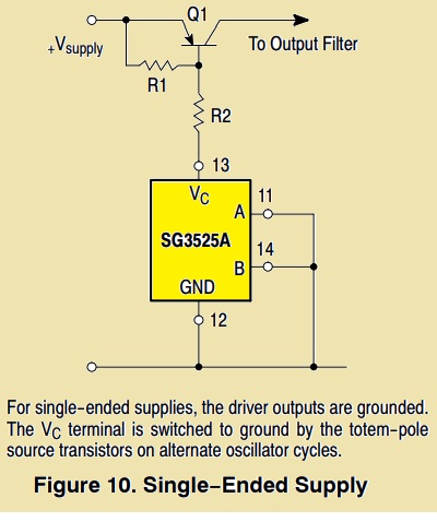
Thanks for this. please recommended values? I don’t understand “to output filter”?
Please ignore the “filter” word….you can use the output as the ON/OFF single ended oscillator.
Yes sir, thanks, please value for R1, please how can I use npn transistor instead of PNP?
Both the resistors can be 10k, and the transistor can be BC557…
hello sir
whit thankfully for useful explanation
I have a MMA inverter welder use sg3525 card control and I turned it for TIG welder and I need to shot down while weldering for this option i used a key for connecting pin 10 to 16 after a few times TIG weldering the Igbt went to die (😂)so pls tell me why and if help me to understand how I should
thank you
shahab
podes probar las mediciones del IC 3525 16 pines porque tengo uno y no se si mide bien los pines gracias
Hello Shahab,
Connecting pin#10 to pin#16 or the positive supply should shut down the IC output, so that should not cause the IGBTs to burn, but maybe due to the sudden voltage spikes the IGBTs are getting affected.
Make sure to use resistor across gate/emitter of the IGBTs, connect reverse diodes across the collector/emitter of the IGBTs, and consider using an IGBT rated to handle 2X power than the load power.
UC3525 Half bridge converter output voltage increases 2V, to 3V from set voltage
sir please can you help me out with the formula solving
sir i want laminating transformer full data.
You can refer to the following article:
https://www.homemade-circuits.com/how-to-make-transformers/
swagatam sir i want 7amp18vdc to 14vdc regulating power supply for lead acid battery charging
You can try any LM338 based power supply. Use two LM338 in parallel.
ckt diagram pls sir
Please refer to the LM317 based circuit, replace the LM317 with LM196 or use two LM338 in parallel:
https://www.homemade-circuits.com/how-to-make-current-controlled-12-volt/
hai sir i have one drought ,sir can run 24v operating voltage inverter transformer, to 12v.
sreenivasulu, I cannot understand your question.
24v operating inverter , can run 12v operating supply, in case 24v inverter secondary side winding modification , i mean 12 0 12v,
24V inverter cannot run on a 12V battery, for modification, rewind the DC side winding to 9-0-9V
it will runs 12v sir
I have tried this IC synchronization many times but the output results remain unstable
if you run a 24V transformer with 12V then the output will be 50% lower.
swagtam sir if 1000w inverter trasnsformer priymariside turns reduced i mean 230v turns data ,reduced 60v will increase amps. can i give e bike operating voltage 60v, 18amp.
Yes it will increase the amps proportionately.