In this post I have explained the pinout function and other important specifications of the IC 4043. I have explained about the complete datasheet of this very interesting chip.
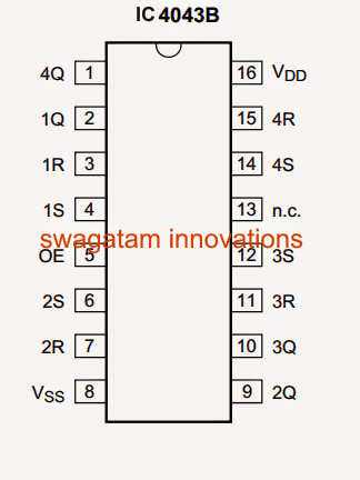
Pinout Datasheet of IC 4043
Technically the IC 4043 is a quad set/reset (R/S) latch with 3 logic state output.
To be more precise this chip has 4 sets of inputs (meaning 8 input pinouts) and 4 corresponding single outputs.
The 4 sets of inputs consist of 4 pairs of set/reset inputs.
For every set/reset we have one corresponding output.
All these set reset inputs respond to high logic signals, creating a bistable effect at their corresponding output pinouts.
Bistable Flip/Flop
Bistable refers to flip flop action, in other words a high pulse to the "set" input makes the corresponding output high from its original low state, and a high to the reset input reverts the above state from high back to low state.
Therefore basically to make a corresponding outputs high, we need to apply a high on their "set" inputs and to make the outputs low again we simply need to apply another high to their reset inputs.
The functioning of the input and output pinouts are as simple as that.
In addition to this, the IC has another interesting input pinout OE which is a common output enable pinout.
Set/Reset Function
For enabling the above explained set/reset actions in the IC, this OE input should be connected with logic high or simply with Vdd (supply votage).
In the above situation the output is allowed with the specified flip flop functioning.
If the OE input is connected with ground, the output freezes and produces a high impedance response, that is neither shows a low output nor a high, rather locks input a unresponsive blocked state, hence the name 3 logic state output.
Thus the OE input can be used to shut down the IC functioning if required for a particular application.
The IC works best with supply voltages from 5 to 15V.
Let's summarize the input output pinout functions and specifications of the IC 4043 with the following data:
- 1Q to 4Q (Pins: 2, 9, 10, 1) 3-state buffered latch output
- 1R to 4R (Pins: 3, 7, 11, 15) reset input (active HIGH)
- 1S to 4S (Pins: 4, 6, 12, 14) set input (active HIGH)
- OE (Pin:5) common output enable input
- VSS (Pin: 8) ground supply voltage
- N.C. (Pin: 13) not connected
- VDD (Pin: 16) supply voltage
More Updates:
In this posts I have explained the working of the IC 4043 and IC 4044 by studying the various specifications, datasheet of the devices and their pinout arrangement.
Basically both the variants are quad cross-coupled CMOS 3-state R/S or Reset/Set Latches. Quad means having 4 outputs which can be set or latched with a logic high through a control input signal, or reset to logic zero by a subsequent input signal.
The 3-state feature allows the ICs to be controlled using 3 logic
The basic working principle of IC 4043 and IC 4044 is the same as above, the only difference being, IC 4043B are quad cross-coupled 3-state NOR Latch, and IC 4044B are quad cross-coupled 3-state NAND Latch.
Pinout Diagram
The following pinouts diagrams of the ICs show the internal structure and pinout details of the devices:


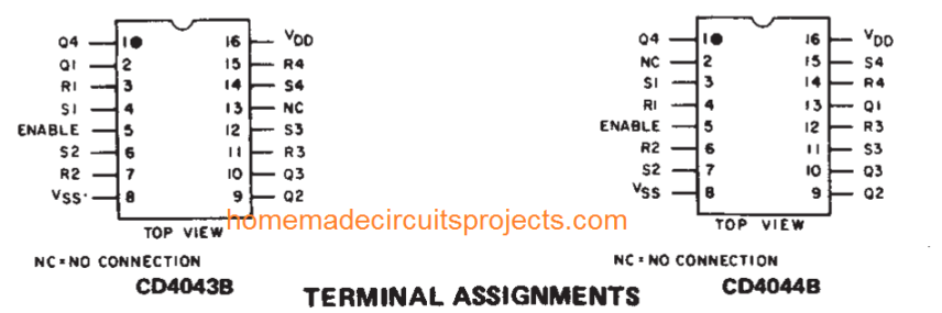
In the diagrams above we can see that each of the types has 4 latches with one output and 2 individual RESET/SET inputs. The function of the ENABLE pin for all the SET/RESET inputs is identical.
A logic HIGH at the ENABLE pin allows the latch states to get connected with the relevant outputs, a logic low or 0 disconnects the latch states from their outputs causing a complete open circuit across the outputs.
NOR Latch, NAND Latch Equivalent Logic Diagrams
The following diagrams show the equivalent latches in the form of NOR and NAND latches, which are present inside each of the 4 latches of the individual ICs.

As we can see, each of the latch blocks are controlled using 3 logic control inputs, namely SET, RESET, and ENABLE, therefore the output is dependent on these 3 input states. The truth table for these 3 logic states can be learned from the following diagram:

In the above truth table, the full-form of the various abbreviated symbolic alphabets can be understood as given below: S = SET Pin R = RESET Pin E = ENABLE Pin Q = OUTPUT Pin OC = Open Circuit NC = No Change
Main Features of the IC 4043, and IC 4044 are summarized below:

Practical Basic Working Simulation of the SET/RESET and ENABLE Pins

Working Description
From the above simulation GIF we can understand the working of the quad latch modules with the following points:
When the SET is pin applied with a positive supply, the output goes high and becomes latched even if the positive potential is removed from SET pin, as indicated by the red LED (forward biased).
When the RESET pin is applied with a positive pulse, the latch breaks, and the output goes LOW permanently even if the positive is removed from the RESET pin. This is indicated by the illumination of the blue LED.
The above operations can be implemented only as long as the ENABLE pin of the IC is at a positive supply potential. When attached to a negative or ground potential, the output of the latch becomes open and unresponsive to the SET/RESET operations.

Comments
Hello Swagatam.
I think I have a clear understanding of my questions concerning above post.
Actually I need above circuit to control a clean, distorted and more audio signal from a preamp, and I will be able to control each audio signal. Is there a way to do this please with the above circuit because I dont know if the Ic can take in audio signal.
Hello Jeremiah,
I don’t think the above ICs can be used for your mentioned application.
Instead the following IC might help:
https://www.homemade-circuits.com/how-to-connect-ic-4066-in-a-circuit/
Thank you so much or the recommendation, it really helpful, With the 4066 it looks like to select or to get an output the button has to be pressed on hold, Is there any circuit i can use with it to make it keep using the output with holding the switch button, Though I know of same CMOS family can be used with it 4017 circuit. But I really don t know ways to combine the two circuit.
I will appreciate any help, recommendation.
Thank you for your time.
Yes 4017 IC can be used to switch and hold the 4066 IC control pins, but the 4017 IC will also need an external clock signal at its pin#14 to move its output sequentially, so I am not sure how to configure it for your application.
Hello sir, It good to find the class available here.
It always a class to count on, Legit !
I have quite little knowledge about 74C373 latching IC, which is better ?
Right now I want to integrate Latching system into an audio circuit with more than 4 effect sections, where the input produce a mix output of one of the effect section
Can I use 2 or more CD4044 IC since I need more than 4 to switched though not at once.
as in the following order.
To use
1) Bypass
2) One and only one out of 4 possible modes
e.g a-mode b-mode c-mode d-mode
3) I want additional mode, When one of the 2 modes is selected.
X mode on/off
Y mode on/off
Though all the circuit will be in same container.
If you my explanation is clear enough I will appreciate suggestions or advices
Thanks for your usual assistance
Hello Jeremiah,
I think it is possible to use more than one IC 4044 for your application. Just make sure their supply lines are fed from a single common power supply.
Hi, I wanted to confirm that this cd4044 keeps the memory of the acquired bit even if I remove the power. I tried and it works as memory.
Hi, I don’t think that’s possible….no CMOS IC has the ability to retain memory after it is switched OFF
I am facing a problem with 4043. Keeping Enable high and auto reset high for a 1 seconds with power up still without the high pules on the set pin output gets ON and at latched status till the reset PIN high.
Can you define why it is happens and how it can be solved.
It will difficult for me to troubleshoot it without a practical testing. If your IC is not working as per the last diagram, then something may be not right with your IC or the power supply.
Sir can i use CD 4043 and CD4044 as a timing circuit for power inverter. Is it possible.
Obinna, you will need an external oscillator to trigger the RS latches, only then you can apply the IC for a power inverter
Buenos dias amigo los felicito buenos circuitos, espero que esten todos bien y mucha suerte.Saludos.
Gracias!!