In this article I have explained the main features, specifications and datasheet of the IC 4033 through a detailed technical analysis.
Electrical Characteristics
- Supply voltage range: 3V to 18V
- Input voltage range:
- Clock input: 0V to VDD
- Display enable input: 0V to VDD
- Ripple-blanking input: 0V to VDD
- Operating temperature range: -40°C to +85°C
- Quiescent current: up to 100 nA at VDD = 18V and T = +25°C
- Maximum clock frequency: 8MHz (typical) at VDD = 10V
- Input capacitance:
- Clock input: 10pF (typical)
- Display enable input: 5pF (typical)
- Ripple-blanking input: 5pF (typical)
- Output drive capability:
- Sink current: 5mA (minimum)
- Source current: 0.4mA (minimum)
- Propagation delay:
- Clock input to any output: 45ns (typical)
- Ripple-blanking input to any output: 45ns (typical)
- Power dissipation:
- Quiescent power: up to 1.8mW at VDD = 18V and T = +25°C
- Maximum power dissipation: 500mW
- ESD protection: 2000V (minimum)
How IC 4033 Works
The IC 4033 is another Johnson decade counter/decoder IC specifically designed for working with 7 segment displays.
Basically it’s a clock or pulse counter IC which responds to positive pulses at its clock input and decodes it serially to produce a directly readable display of the count number through the connected 7 segment display module
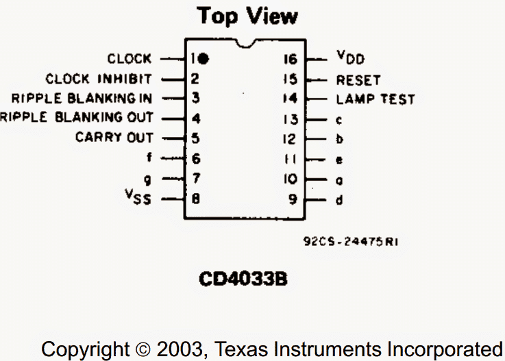
Pinout Specification of IC 4033
Let’s try to understand how to use the IC 4043 by knowing the functions of its pinouts:
Pin#1: It’s the clock input pinout of the IC, which is assigned for accepting positive clock signals or the pulses which needs to be checked or counted.
Pin#2: It’s the clock inhibit pinout of the IC, As the name refers to, this pinout could be used for inhibiting the IC from responding to the input pulses by configuring this pinout to the positive supply or the Vdd. Conversely in order to allow normal functioning of the IC this pinout should be grounded.
Pin#3/#4: These are the Ripple blanking IN and Ripple blanking OUT pinouts of the IC, which provides the user with the option of either allowing the non-significant zeros to be displayed or to be left out from the connected digital displays.
For example suppose you have cascaded 8 nos 4033 ICs for reading 8 digit displays and have reached a reading of say 0050.0700.
Expressing this number as 50.07 makes more sense than 0050.0700, for implementing this we need to assign pin3/4 which are blanking IN and blanking out respectively in a certain unique manner across the 8 ICs.
To understand the procedure we’ll need to take account of the digits which is most significant in the order, and which is least significant.
Automatic non-significant Zero Suppressing
In the number 0050.0700, the most significant digit on the integer side is “0” in between 5 and the decimal, conversely in the fractional side the least significant digit is “0” at the extreme right.
For enabling the RBI and the RBO (pin#3/#4) correctly on the integer side, we need to connect RBI of the IC associated with the most significant digit to a low logic or ground and the RBO of that IC to the preceding lower significant IC’s RBI.
This should continued until we reach the first IC associated with the extreme left digit of the integer side.
Now for suppressing the non-significant zeros at the fractional side, we need to connect the RBI of the IC 4033 associated with the least significant display to ground and connect its RBO with the previous IC’s RBI, and continue this until we reach the extreme digit of the display situated just before or just at the right side of the decimal point.
The above feature of the IC is called automatic non-significant zero suppressing.
However if the display is intended to display a purely fractional number, then the RBI pinout of the IC associated with the display that’s touching the decimal point on the integer side must be terminated to the positive supply. For example, for a number 0.7643, the IC associated with “0” must be tackled as explained above, same for the IC associated with the digit “0” for the number 764.0
The above feature of suppressing non-significant zeros might look “insignificant” however the feature heps to save “significant” amount of power and becomes incredibly useful for applications that employ battery as the power source.
Pin#14: It’s the “lamp test” pinout of the IC. As the name signifies it is used for testing the connected digital displays in terms of illumination level.
When this pinout is connected to a high level or the positive supply, the normal function of the IC is disabled and all the digits of the 7 segment display are applied with a high state so that the digits are allowed to get illuminated together.
This allows us to test the intensity levels of the digits and if any of the display digits are not functioning optimally or are dim due to some malfunction.
Pin#6,7,9,10,11,12,13: All these pinouts are the outputs of the IC which are configured with the discussed 7 segment digital display module.
Pin#15: It’s the reset input of the IC, a high logic or applying the supply voltage to this pin resets the IC completely, resulting in clearing all the data from the display and restoring it to zero.
Pin#5: It’s the carryout pinout of the IC, it sends a high logic output after every 10 legit clocks at the clock pin#1 of the IC. Thus pin#5 is used as a clock output or a carry forward extension for the next corresponding IC 4033 when many of these are cascaded together in a multi-digit display counter systems.
Pin#16 is the Vdd or the supply input of the IC.
Pin#8 is the Vss, or the ground or the negative supply input pinout of the IC 4033.
The IC works best with supply voltages between 5V and 20V.
Main Features
- Decade counter/divider with decoded 7-segment display outputs
- Display enable and ripple-blanking input
- Fully static operation
- Medium-speed operation: 8MHz (typ.) at VDD = 10V
- Standardized symmetrical output characteristics
- Quiescent current account to 100 nA
- High noise immunity: 0.45 VDD (typ.)
- Low power TTL compatibility: fan out of 2 driving 74L or 1 driving 74LS
- Medium size DIP package.
Applications
The IC 4033 is a decade counter with decoded 7-segment display outputs. It is commonly used in electronic circuits as a driver for 7-segment displays in a wide range of applications, including clocks, timers, scoreboards, and other electronic displays. Here are some examples of how the IC 4033 can be used:
- Digital Clocks: The IC 4033 can be used to build digital clocks. By connecting the clock input of the IC to a 1 Hz clock source, the IC will count from 0 to 9, and the output will drive the 7-segment display to show the digits of the clock.
- Scoreboards: The IC 4033 can be used to build scoreboards for games and sports events. By connecting multiple ICs in cascade, the circuit can count from 0 to 99, 0 to 999, or more, depending on the number of ICs used


Comments (4)
Can ICs 4033, 4017 and 4020 be used interchangeably?
They cannot be interchanged since their pinout assignments are different.
Hi, great explanation of 4033 operation – very helpful.
How do I configure the second cascaded 4033 to carry-on on the 6th clock signal instead of the 10th?
In other words, so I can use 3 displays in total to represent seconds and minutes.
If I leave second display to carry-on on 10th clock signal then I will have duration expressed as total number of seconds. Would rather have minutes and seconds, hence 2nd display must carry-on on 6th clock signal.
Thanks Tim, Glad you liked it.
however, since it was written a long time ago and I have totally forgotten its working details, so it will be difficult for me to revise the details again.
But I have a related post which you can probably refer to and get the required solutions from it. Here’s the link:
https://www.homemade-circuits.com/cascading-ic-4033-in-multiple-digit/