MOSFET based amplifiers as we all know are outstanding with their sound qualities and they can easily beat the performance of other counterparts based on power transistors or linear ICs.
Why use MOSFETs in Amplifiers
Amplifiers based on mosfets are not always easy to design or make.
Moreover after assembling a prototype, testing to perfection always remains an issue with new electronic hobbyists.
You might have come across many hi-fi complex mosfet amplifier designs, but might have not dared making it just because of the above reasons.
The simple mosfet amplifier circuit diagram is super simple to build and yet will provide you with a crystal clear 100 watts of raw music power that all the listeners will cherish for a long time.
The idea was developed a long time ago by the Hitachi researchers and still it remains one of the favorite designs of all time considering the involved simplicity against quality.
How the Amplifier is designed to Function
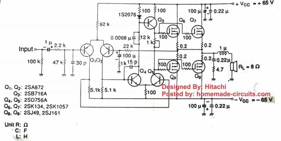
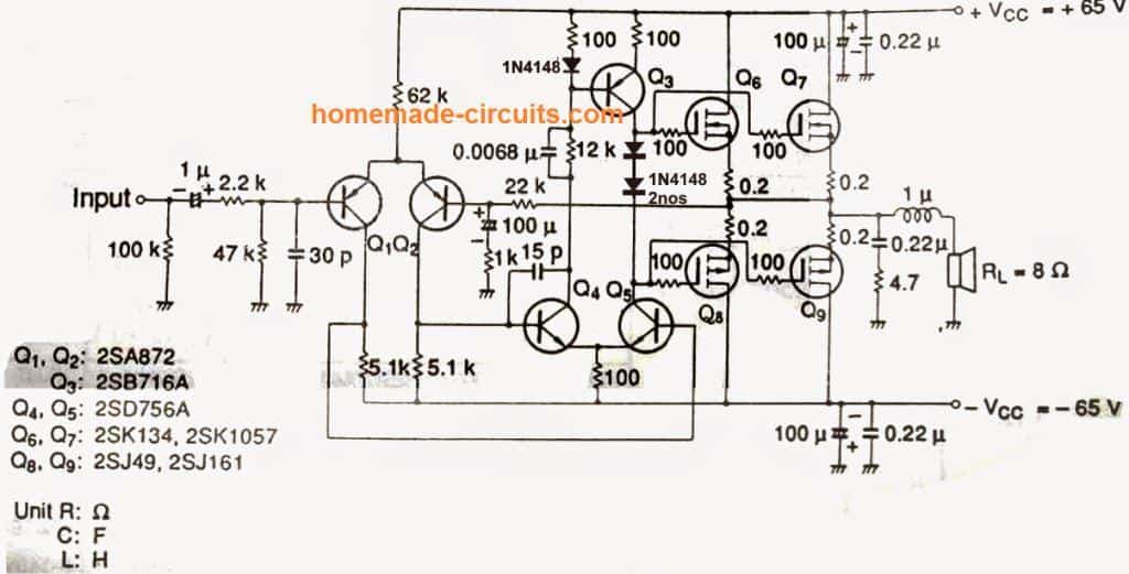
Looking at the figure we can understand the circuit with the following points:
- The involved simplicity would also certainly mean that some of the ideal features of the circuit was sacrificed in the design, for example it lacks a constant current source for the differential amplifier at the input stage of the amplifier.
- But this has no serious impact on the design, whatsoever..
- The differential amplifier makes sure that the input is sufficiently amplified to some reasonable levels suitable for feeding the next driver stage.
- The driver stage consists of a well balanced high voltage transistor stage which are necessarily positioned for driving the output power mosfets.
- The pot positioned in between the two sections of the driver stage is used for setting the quiescent current of the circuit.
- The output stage is a common push pull type of mosfet stage which finally provides the boost for amplifying the fed low signal music into a 100 watt thumping music over a 8 Ohm speaker.
- The shown parts might be obsolete today so may be replaced as follows:
- The differential transistor may be replaced with BC556.
- The driver transistors may be replaced with MJE350/MJE340.
- The mosfets may be replaced with 2SJ162/2SK1058
The below given diagram is the original design from Hitachi, see the preset arrangement for setting up the quiescent current. You must adjust this preset to set the quiescent current to zero before connecting the speaker.
I have modified the above design by adding a couple of 1N4148 diodes in place of the preset. This gets rid of the preset adjustments and allows the user to directly switch ON the amp with a speaker connected.
Parts List
Resistors
All resistors are 1/4 watt, CFR 5%, unless otherwise stated.
- 100 Ohm = 7nos
- 100k = 1no
- 47k = 1no
- 5.1k = 2nos
- 62k = 1no
- 22k = 1no
- 2.2k = 1no
- 12k = 1no
- 1k = 1no
- 4.7 ohm = 1no
- 0.2 ohm / 5 watts = 4nos
Capacitors
All capacitors must be minimum 100V rated
- 1uF = 1no Electrolytic
- 100uF = 3nos Electrolytic
- 15pF = 1no Polyester
- 30pF = 1no Polyester
- 0.22uF = 3nos Polyester
- 0.0068uF = 1no Polyester
Semiconductors
- Q1, Q2 = BC546
- Q3 = MJE350
- Q4, Q5 = MJE340
- Q6, Q7 = 2SK1058
- Q8, Q9 = 2SJ162
- 1N4148 = 2nos
Misc
Inductor = 1uH, 20 turns of close wound 1mm super enameled copper wire, with 10mm diameter (air core)
Note: The resistor, and capacitor values are not critical, slight up and down will do, and will not cause any harm to the performance of the amplifier
Parts, PCB Images and Prototype
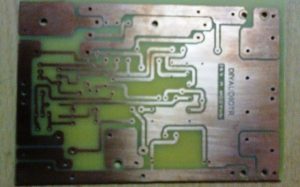
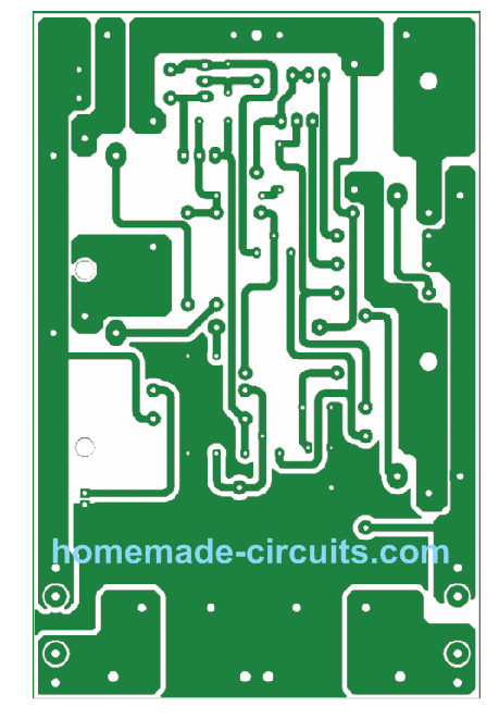
1) The first image shows the PCB which was used for the 100 watt mosfet amplifier circuit project
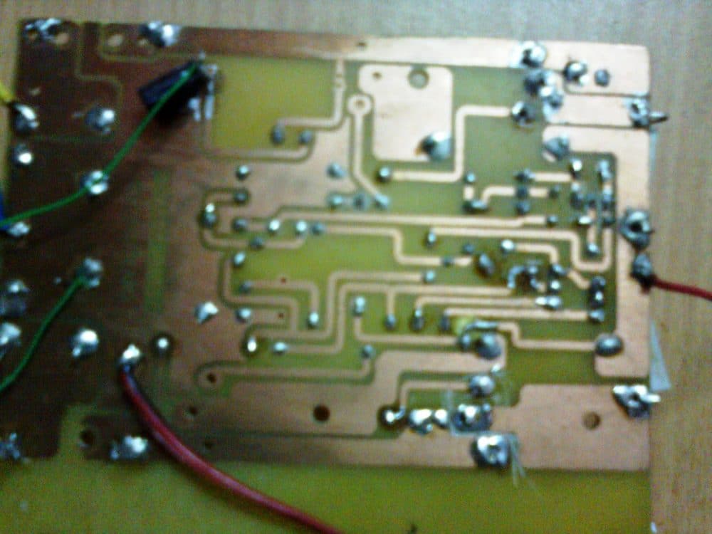
2) The second pic shows the soldered portion of the assembled circuit.
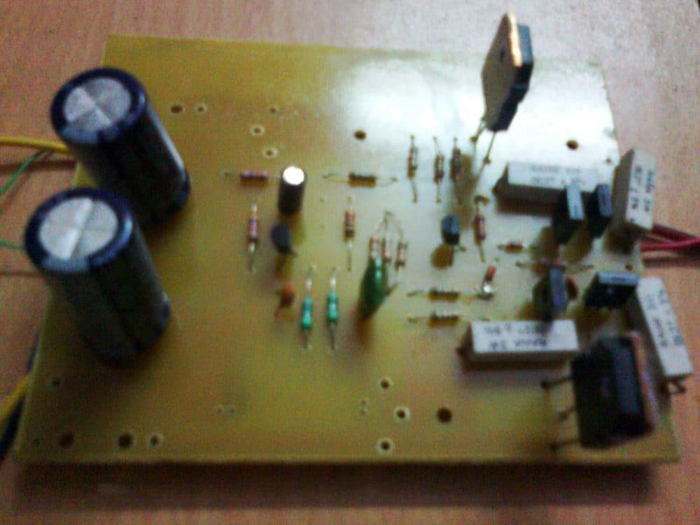
3) The third pic illustrates the components side of the assembled board
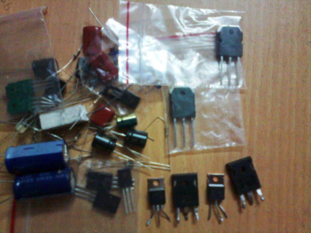
4) The fourth image relates with a few of the components involved with the the circuit making.
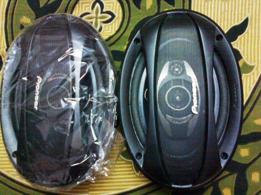
5) The fifth figure witnesses the speakers which was used for testing the amplifier with astonishing levels of clarity and superb power outputs :p
I used only a couple of mosfets which could generate power outputs well over 100 watts RMS, connecting more numbers in parallel can easily enable this circuit to cross beyond the 1000 watts mark.
If you are intending to buy a ready made power amplifier for your home, I would suggest, you build this one instead and be the proud owner of this outstanding home built power amplifier unit which would probably serve you for years.
The Design which I Built
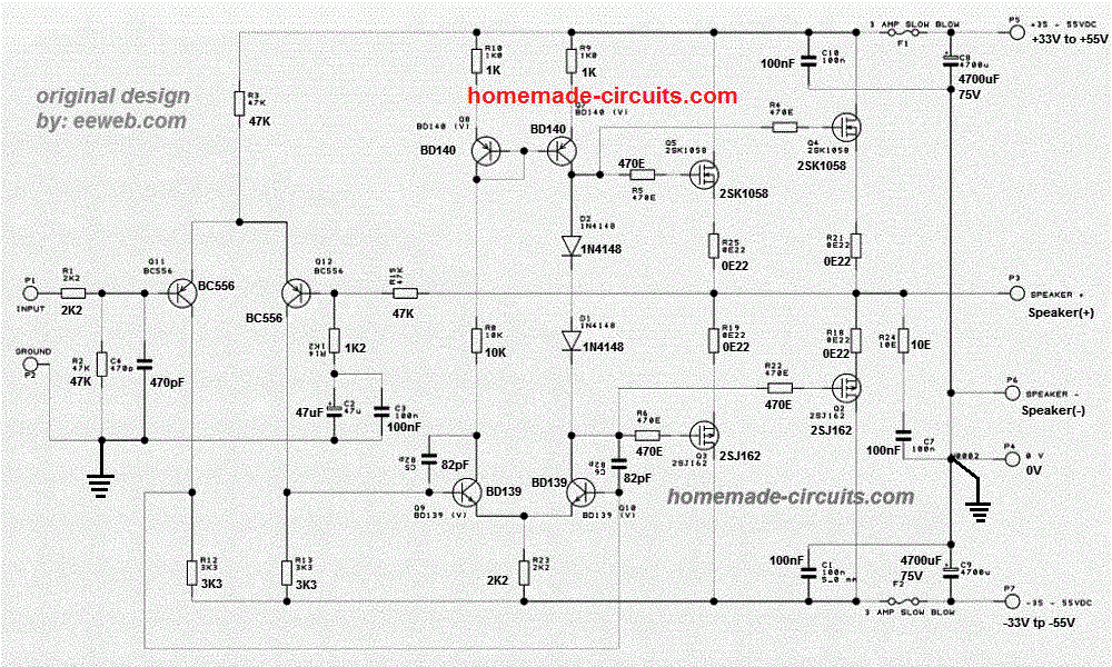
The circuit which I tested was taken from eeweb, and the diagram is shown below. It is similar to the above original design from Hitachi. However since this is the one which I have tested I would recommend you to go with this one.
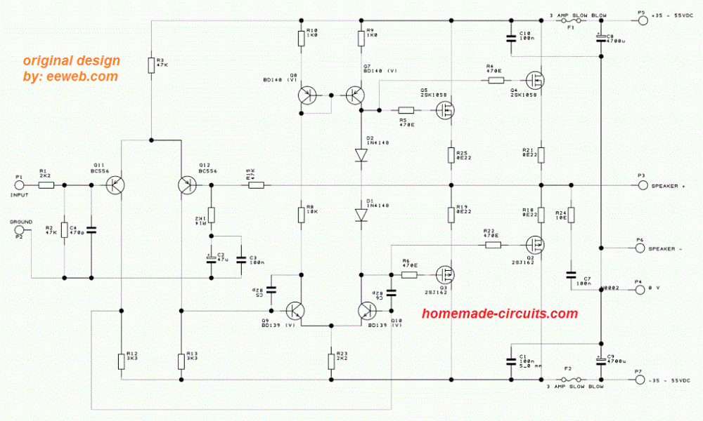
Circuit Diagram with Magnified Part Values
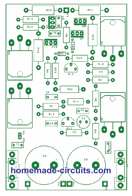
PCB Track, and Component Layout Diagrams
Credit to the Original Creator
PCB Dimensions are 120 mm x 78 mm



Questions & Answers
Hello,
first of all, thank you for the blog!
My question: could we run a +-100v psu directly on this pcb?
Hi, as per the voltage specifications of the transistors, a maximum of 60 V can be used. You can perhaps try replacing the BD transistors with MJE variants and then use 100V.
The first circuit is not working…am using 22vac secondaries, but am having constant voltage in my speaker stressing it and too much humming…
The first circuit was designed by Hitachi engineers, so it should work.
You can try the last circuit instead, it has been tested by me thoroughly. Make sure to use the PCB design for assembling.
Hallo Erstmal, wie wird bei dieser Platine der Kühlkörper montiert? Oder laufen die Mosfet ohne Kühlkörper?
Hi, heatsinks are definitely required for the MOSFETs, you can put individual, standalone heatsinks for each of the MOSFETs, such as this one:
https://www.homemade-circuits.com/wp-content/uploads/2019/11/78xx-on-heatsink.png
Hello dear,i need power suplly 12v to 55v for your circuit on car amp,can you help me?
Hi, you can try the first circuit from the following article. You will have adjust the zener value and the coil winding to get the required results correctly.
https://www.homemade-circuits.com/12v-car-laptop-charger-circuit-using/
There is no specifications on this project, what were the original Hitachi specs , if you know?
I would like to build it, can you supply/sell PCB?
Regaeds,
Tomo
The wattage specification will depend on the supply voltage used. Wattage = Supply voltage x 3 amp. Max voltage for the first two circuits should not be over 60 volts.
I would recommend building the last design since it is a tested one….and the wattage range can be as high as 300 watts.
Sorry…I don’t have the PCBs for this design.
please is the 2Sk1058 and 2SJ162 THE output Transistors ? and please if I replace the BD Transistors with Mje 340 and Mje 350; and I Replace the BC556 with 5401 . would it take up to 200v. because the transformer i have it’s a Center Tap transformer with a 100v-0-100v Ac output.looking forward to hearing from you . Thanks .
Yes those are 2Sk1058 and 2SJ162 MOSFETs.
Sorry, 200V would be too high…you can at the most use 120V DC, nothing above that….
And lastly. is there a way you can use only N-CHANNEL MOSFETS for the output stage.E.g IRFP260N
No sorry… the design should be exactly as given in the above article…
please can I replace the mosfets with these Mosfets.IRFP260N and IRFP9240? N-and-P Channel
If these are rated with 150V VDS then you can use them
ok Thanks . They actually Rated
200 VDS . BOTH.
IRFP260N and IRFP9240.
I really appreciate your kindness
Great, then it is absolutely fine, you can use them.
Hi Swagatam
I decided to install two fuses in my Trace Elliott GP7SM 130 power amp in the + & – power rails by cutting the traces and soldering wires to chassis mounted glass mini fuse carriers so as to make the measuring of the currant draw easier but I am confused as to how to properly set the quiescent current for this amp that uses 1 x 2SK135 & 1 x 2SJ50 lateral MOSFET’s.
The supply voltage to the main power amp with no pre-amp input connected reads: 143 Volts & 75 Volts + or – either side of chassis/ground.
I took a reading across the speaker terminal output with no load which reads: Approx. 35-mA, although that voltage reading does jump up and down a few mV’s while testing.
I read somewhere that to adjust the quiescent current correctly I have to short the input to chassis /ground so there is no signal entering the amp, insert a 4 Ohm load resistor (4 Ohms is the correct load for this amp) then set the multi-meter to 10 Amps on the positive rail and adjust the pre-set pot until no currant is drawn, however I have also read that the Mosfets on this amp should be set to be drawing about 100mA’s??? Help! I am confused!
Am I mixing up quiescent load with bias load and the need to insert a load resistance?
I have asked Trace Elliot if they sell an actual service manual that explains the correct procedure to set this amp up properly but they have ignored my requests.
Any help Swagatam would be much appreciated.
Kind regards “Confused”
Stefan
Hi Stefan, my idea of setting quiescent current is by connecting small flashlight bulbs in series with the positive/negative supply rails, and then adjusting the preset until the glow on the bulbs just disappear.
Yes you much short the input terminal with the ground, while doing the above setting up process.
Thank you Swagatam
I saw that somewhere on the web but couldn’t find it again and needed to know what size tungsten lamps to use.
I have heard they should be 1.2 watt 24 volt dc types!?
Are 3 volt flashlight lamps OK? Also do I have to have a load connected to the speaker terminals i.e. 4 ohms as the amp is designed to use, I only have an 8 ohm power resistor at the moment but could order a 4 ohm?
Regards
Stefan
Hi Stefan,
In my design I had used low current incandescent bulb which are normally used in 220V mains string lights. They are tiny around a cm long. Ideally the voltage of the bulb should be equal to the supply voltage of the amplifier, however practically a 24V bulb will also work nicely. The current spec of the bulb must be low, at around 100 mA.
3V flashlight bulb might not work according to me, they might burn at supply volts over 12V
Yes 8 ohm speaker load will do temporarily.
Thank you Swagatam
Much appreciated advice
Kind regards
Stefan
You are welcome Stefan.
Hi
I am looking to build this design, on the originals there’s an inductor before the speaker but on the tested designs there isn’t, what’s the reason for this and can I add one ?
Hi, The first two designs and the last design are not the same. The coil is used in the first two designs, it is not required for the last design which I built and tested.
Hi
Thanks for the reply. I will build up this circuit and test
What’s the power requirements per rail, will 3A be suitable?
No problem, please go ahead.
3 amps at 35 V, or 50 V will be fine for this amplifier
Hi Swagatam
This Hitachi circuit was and is obviously a very popular circuit and used in many Hi-Fi amps, in the 90’s the same circuit was used in a Trace Elliott GP7 SM bass amp combo, I have just part repaired a very badly bodged one for a friend and was stuck on how to set the quiescent currant correctly.
The Trace Elliott amp PCB board doesn’t really make it easy to temporarily install a couple of 100mA lamps to test the quiescent current temporarily so I was very interested in your diode modification but I was little disappointed that you didn’t include an explanation as to how this modification works and for the better but also if it would work in all types of amps including a Trace Elliott bass amp, also, I wonder why this diode method wasn’t used in the original design as surely two diodes are cheaper than a pot!
As you can imagine, this circuit would be driven very hard in a bass amp combo so I was worried that your diode modification may not be the best way to go.
Sorry if the above post appears to sound negative, it’s not my intention to offend.
Anyway your/this article is a great help even if I eventually go with the lamp method… Thank you!
P.S. While searching for pdf schematics and details of the GP7 I discovered a guy called mimi2008 who did a redesign of the original Trace Elliot GP7 PCB board, he moved a few components including the cooling fan supply arrangements.
I am looking at changing the cooling fan supply to either a 12 volt regulated “Heat dissipation” or a “PWM Controller” albeit only if the switching MOFET doesn’t induce noise into the amp although I guess that can be addressed with a cap or two as I find the original 270-Ohm voltage dropper resistor feeding the fan to be a bit Neanderthal for these times.
Unfortunately I can’t remember which site it was on but I have a pdf file of the board and circuit if anyone wants a copy.
Sorry for the war and piece post.
Kind regards
Thank you Stefan, for the detailed information! The two diode idea is not mine rather taken from the last circuit from the above article. I have not provided the explanation since I am myself not sure how the two diode idea helps to eliminate the preset. If I happen to figure it out I will surely update it here for you! If you are finding the resistor voltage dropper a bit Neanderthal, you can very well try using a buck converter instead, that would be a very efficient approach.
Good morning Swagatam ,
Is there any other ways to adjust the preset without the `rice bulbs`? I Cant find any rice bulns,so this option is a non starter for me.
Thank you .
Ernesto, the quiescent current adjustment is recommended only for the first design, not for the last design. Using small low current bulbs in series with the supply lines is the best method to adjust the quiescent current for amplifiers. You can try any small bulb, rated at around 100 mA current.
Hello, Sir,
Hope you are safe.
I have made the amp based on the last diagram,and am having some challenges as below.
with parts – BC640 , MJEs and 2 *4148
1.There is voltage at input pins of Mosfets thru the 470ohms resistors.
PSU 18 0 18 and on d1 & d2 there is 17.4 volts ,Thus a drop in approx 2v.
2.There is voltage also on the output(speaker out terminal) this drops to zero when i connect a speaker.
3.mosfets irpf450 and 9240 pair, there are failing a minute after i power up , they are heating up excessively .
4.Without the mosfets, there is a good audio buzz sound if i touch the input pin on the amp -with a small 5w speaker.
Kindly advise me on corrections.
Thank you in advance for your time and efforts.
Hello Ernesto, as far as my experience goes, the last design is a plug-and-play kind of design, in which nothing can go wrong. When I built and tested it, it started working superbly without any initial adjustments. I was amazed with its crystal clear sound output and flawless amplification.
Did you build it over the recommended PCB? Any other option might lead to errors and complications.
I think you should initially try the exact same MOSFETs as suggested in the article, just to be sure that everything is as per the diagram.
Hello Swagatam,
Thanks for your response,
Other wise I have to re-do my work.
Confirm we should not be getting any dc on the speaker output terminal?
Thank you.
You are welcome Ernesto, yes there should be no continuous DC across the speaker terminals.
Thank you sir for the link I appreciate sir
You are welcome Muhammad!
Thank you sir for the quick response.
As I have understood, amplifier is composed of three main stagess.the preamplifier stage,the driver stage and the final out driver stage am I right sir? If I know the current and voltage specs of every stage I think I will be able to build my own amplifier from scratch,I will be glad if u could tell me or refer me to a link that explains in detail all these parameters. Thank you once again sir.keep up the good work.
No problem Muhammad, I have a related post which you can refer to, it might help you to get some useful info regarding amplifier designing.
How to Design MOSFET Power Amplifier Circuits – Parameters Explained
Hi sir, God reward abundatly for the great job u have been doing. Regarding this amplifier I have a question. The above modified circuit been a mosfets amplifier,the voltage across the two diodes will be 1.4v right? If so,
1. is this voltage enough to drive the mosfets into saturation? Since mosfets require voltage not less than 2.5v base voltage to saturate.why I ask is because I once tried replacing mosfets with BJTs in a similar design an I got a cracking sound at low volume but with high volume,the sound becomes clear.this does not happen with the BJTs connected,so I totally may be the voltage across the two diodes in series wasn’t sufficient to drive the mosfets at lower volume pls is my assumption true?
2 I have seen many amplifier circuits having this kind of design (with two diodes in series )using BJT as output transistors, does that mean that this amplifier will work even when the mosfets are replaced with BJTs?
Pls sir I anticipate your response thank you sir
Thank you Muhammad, You maybe correct, BJTs require only 0.7 V to switch ON, while MOSFETs require much higher than this, however, in my prototype the amplifier perfectly well even at lower volumes, so I don’t think the two diodes are creating any problems.
You can try replacing the mosfets BJTs, just make sure to replace the base 100 ohms with higher ohm resistors