In this article we are discussing a handful of simple, mini audio amplifier circuits which can be built quickly for amplifying very tiny input signals into audible speaker outputs.
1) 1 Watt Amplifier Circuit
The first simple mini audio amplifier circuit works with a 'complementary' output stage, having a single NPN and a single PNP power transistor, that gets rid of an output transformer commonly observed in older amplifier models.
Power output is around 1W, with fairly minimal distortion. The input signal is transferred via the volume control RV1 and next through C1 to the Q1 base.
The collector load for Q1 consists of R1, R5 along with the loudspeaker.
The collector voltage of Q1 is around 50 % of the supply voltage, i.e. 4V5. The Q2 and Q3 bases are likewise with the identical voltage (pretty much) as the Q1 collector due to the fact the R1 value is very small (68R).
Within the intersection of the Q2, Q3 emitters the voltage may also be almost 4V5, R3 and R4 and extremely small value resistors to control the current passing across Q2 and Q3.
If the amplified input signal is no more than 4V5, Q2 is switched off (since the base will likely be at the reduced voltage compared to its emitter), nevertheless Q3 may continue to pass the signal.
As soon as Q1 amplifies the signal over 4V5 the situation gets reversed, Q2 switches ON and Q3 is switched off.
The signals are mixed at the the common emitter joint of Q2 and Q3, and transferred to the loudspeaker by means of the big electrolytic capacitor C2. Smaller value for C2 capacitor can cause a weak reduced frequency response.
Negative feedback is supplied by R5 and R2, which guarantee stability by minimizing the gain marginally.
R1 is incorporated in order to get a tiny amount of base bias for Q2 and Q3; much more superior layouts make use of thermistors or diodes to protect against thermal runaway situations that could damage the pair of output transistor.
A negative aspect is the transistor's DC coupling, where if one particular transistor shifts its characteristics the effect could be devastating! Because of this, the output transistor pair must be a correctly 'matched pair'.
Some other variants could be tested out given that they too are correctly matched with identical hFE.
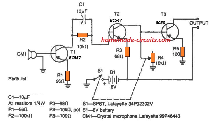
2) Tiny Amplifier for Hearing Aid
When a cheap and dirty audio mini amplifier circuit is what you are looking for, you can probably test out this little device.
Among various other factors, it could be accustomed to increase the output of a headphone for the people with hearing loss.
The circuit is a simple twin transistor, audio amplifier. The 1st transistor, Q1, works like a basic medium gain preamp which obtains its signal coming from C1, acting like a DC blocker.
Transistor Q1 amplifies the signal and directs it to C2. That transistor}, next, feeds the signal to Q2, which is configured like the power amplifier stage.
This stage amplifies the signal even more, and C3 switches it towards the speaker.
You could possibly find a little bit of distortion, nevertheless this could be minimized through testing with different values of C5, maintaining it within the indicated range. In case this does not work properly, consider some other values.
However thinking of how the gain of transistors can differ, it most likely will need quite a bit of experimenting to have all the things to function rightly.
3) Improved Miniature Hearing Aid Amplifier Circuit
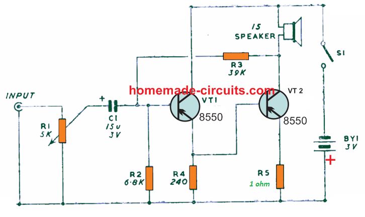
4) Half Watt Amplifier Circuit
The next miniature audio amplifier circuit presented here is quite easy.
The output power is around 250 mW which usually is fairly enough for the majority of applications and it is as good as any typical transistor radio. The distortion amount is pretty high, at around 5%.
This simple small amplifier is moderately sensitive and can provide 100 % output having an input of approximately 50 mV.
Input impedance is approximately 50k. A basic tone control is integrated. Although this is not actually an active tone control, rather than a passive one, the effect is fairly adequate. The volume control center arm is attached to the Q1 base through a DC blocking capacitor.
Circuit Working
Q1 is hooked up like a very traditional common emitter amplifier along with R2 supplying the base bias and R3 behaving like a collector load.
This stage is directly coupled to the second transistor which is a PNP type. By doing this the current getting through Q1 supplies the bias for the 2nd transistor.
With the values employed, the output of the second transistor is coupled straight to the coil of the loudspeaker.
This may not appear to be a wise idea because the standby current in the output transistor constantly biases the coil sometimes a bit in or out from its typical operating level.
Nevertheless if a big speaker is utilized, as it should be, this features hardly any impact and because we are not expecting a great Hi-Fi output, it does not make a difference.
Tone Control
The tone control includes C2 and RV2 that happen to be joined across the collector/base of Q1.
When RV2 is set at a high resistance value, this has hardly any impact but when set at minimum level the 100nF causes a feedback of the high frequencies that tend to be out of phase, resulting in their total cancellation.
In order to to enable the circuit to work correctly R3 should be determined meticulously.
The value indicated in this article is 39 ohms which is just an average range and even though it might work well for preliminary setting up to guarantee the circuit is functioning, the value needs to be determined by experimentation.
In case it is very small you will see extreme distortion on the larger volume configurations.
When it is excessively high the current drain will probably be too much although the quality of the sound output will be very good.
One can find a couple of methods for picking out the value. With no multimeter the value must be determined as being the smallest that is appropriate for decent quality.
In case a multimeter is accessible this should be connected in series with the supply voltage and R3 has to be chosen to ensure that amplifier quiescent current, which happens to be the current operating in the absence of an input signal, is around 20 mA.
It is crucial that Q2 is installed over a heatsink since it can get incredibly hot and can enter into thermal runaway if no heatsink is employed.
The speaker impedance is not really important and in the prototype speakers as low as 8 ohms and as large as 80 ohms almost all performed well. However, altering the speaker impedance might also require a change in the value of R3.
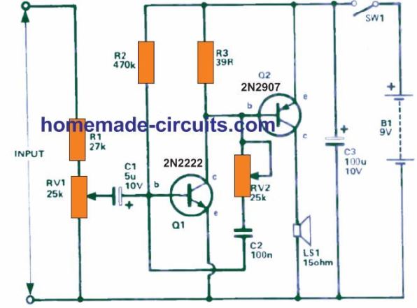
5) Basic 3 V Mini Amplifier Circuit
To decrease the amount of parts, direct coupling is employed in between Tr1 and Tr2 and between Tr2 and the loudspeaker.
Tr1 works like a common collector amplifier loading through a common emitter amplifier Tr2. The Tr1 base bias is extracted from the collector of Tr2. Since this is out of phase with Tr1's base an excessive amount of stabilization is accomplished.
Portion of the standing collector current of Tr1 likewise runs via Tr2 through base to emitter thus delivering the essential bias.
Negative feedback is supplied by R5 and R3. R3 delivers feedback through the two stages and R5 implements feedback through the output to the input of Tr2.
The effect of this feedback results in an incredibly flat response curve down to surprisingly low frequencies.
The high frequency response could be substantially enhanced by changing the transistors with 2N2907. Applying this device may also bring about an boost in gain.
The sub-miniature amplifier circuit may be fantastic for boosting the output from your FM or AM tuner.
In case you have a compact radio, that works only with an earpiece output, it could be accustomed to raise the volume approximately to loudspeaker level. To get this done just hook up the output from your radio on the input of the amplifier.
The loudspeaker, utilized on this amplifier, must be as big as it can be, if at all possible a 12 inch type inside an housing.
Implementing an extremely small speaker can lead to a bit of inefficiency due to the fact that there could be ample current moving over the winding even while the input signal is not available.
The current utilized through the battery is going to be relatively high, approximately 150 ma. which means this must be as large as may be possible.
6) Mini Amplifier Circuit, Working with 3 V
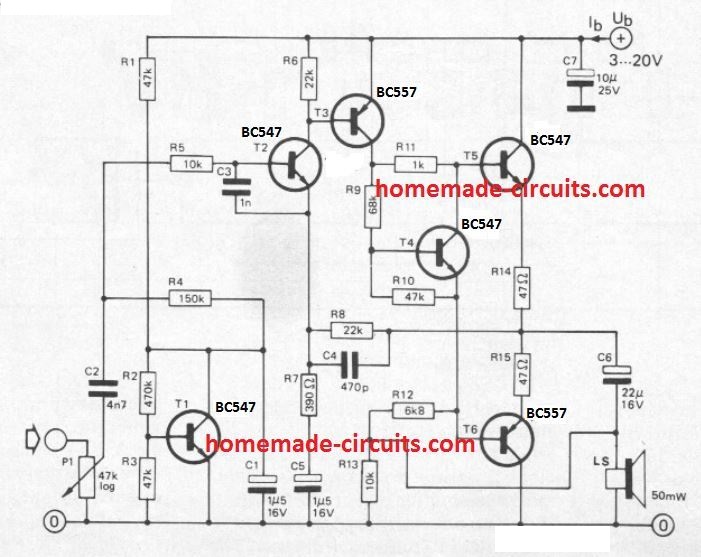
This simple mini amplifier can work without any issues or errors through supply voltages between 3 V and 20 V using source resistances as:
Supply voltage / 2 mA (k ohms)
The power output that the amplifier could deliver is, naturally, determined by the supply voltage and its loudspeaker resistance, as is visible through the enclosed table.
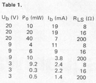
The quiescent current usage of the amplifier is in between 1 mA and 1.5 mA, the precise magnitude dependent on the variety of transistors employed.
If the quiescent current drops beyond this particular limit it will likely be essential to tweak the value of R9. As is evident in the table, the amplifier functions efficiently with high impedance loudspeakers.
Since speakers with impedances as large as 200 ohms cannot be easily available, the choice is to try using a lesser impedance speaker having a complementing transformer.
For instance an 8 ohm speaker may be employed with a transformer using a ratio of around 5:1.
Although the amplifier output power is not very high, it is however adequate enough when combined with a moderately efficient loudspeaker inside a silent area. The amplifier's voltage gain is around 50 and the 3 dB bandwidth is around 300 Hz to 6 kHz.
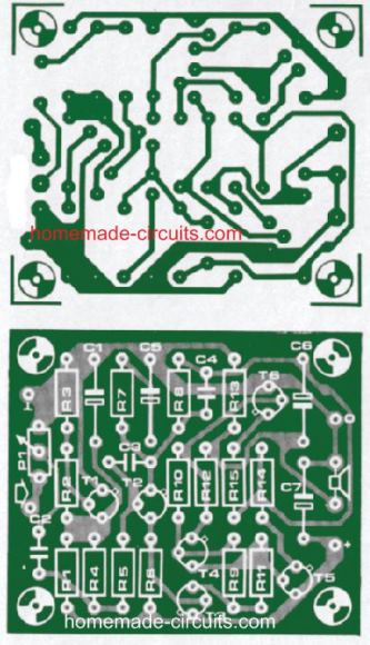
PCB Designs
1.5 Watt Discrete Amplifier
This little amplifier circuit can be an handy support to the any audio experimenter.
It could be accustomed to amplify, and produce audible, impulses via oscillators functioning within the acoustic range, to track signals via a different audio amplifier that may be defective, to amplify some other signal to a acceptable power level for measuring or relay operation etc. etc.
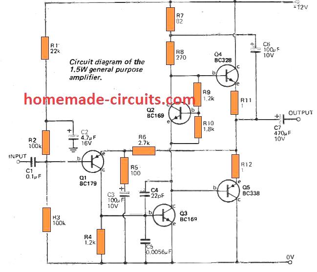
In the modern times, one can find a lot of integrated circuit power amplifiers supplying outputs of 1 to 3 watts although the majority of them demand cautious layout of the circuit so that you can avoid instability (an unstable amplifier might vibrate and become destroyed consequently).
Furthermore, a discrete transistor amplifier is much more informative because voltages could be assessed to get a greater perception of its working.
Hence the present small amplifier is developed applying discrete transistors that apart from being far more steady than IC based designs, is perfectly suited to the requirements of the user.
Transistors Q2, Q4 and Q5 are cemented into a small aluminium that works as a heatsink.
How the Circuit Works
This circuit is pretty typical of a great number of audio amplifiers. The primary voltage amplifier transistor Q3 runs the secondary match (NPN plus PNP) Q4 and Q5 that are buffers delivering large current gain yet lower than unity voltage gain.
For the reason that bases of Q4 and Q5 tend to be appropriately two base emitter junctions aside, Q3 is employed to set the bias voltages for these BJTs.
Transistor Q1 works like an error amplifier that analyzes the input voltage and a divided down variation of the output voltage.
When there is virtually any variation it supplies a control voltage to Q3 so that the error is fixed.
The output voltage is split down through the ratio of (R6 + R5)/R5 and therefore the worked out gain is going to be 28 even though proper gain will likely be somewhat less.
The dc bias point of the amplifier is additionally established by Q2 which is unaltered by R5 and this is separated through C3.
To keep up a roughly constant current in Q3, capacitor C6 is positioned to ensure the voltage across R8 (thus the current through it) constant. Capacitors C4 and C5 are accustomed to offer frequency compensation.
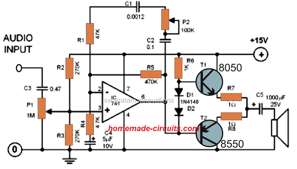
Small Amplifier with High Input Impedance
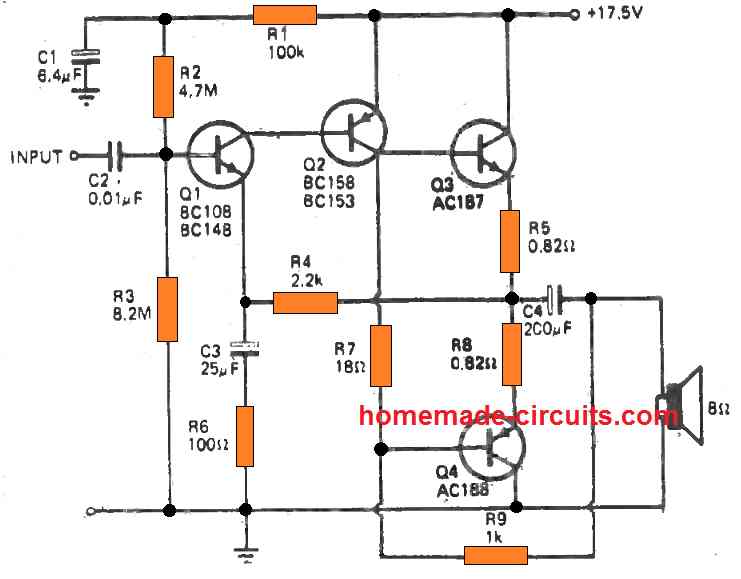
This small amplifier features a high input impedance of 1.1 megohm by ensuring that the Q1 transistor's collector current is held low, and by incorporating a high amount of ac and dc feedback.
The input sensitivity of this simple amplifier circuit is fine-tuned by adjusting the resistor R3 value.
The circuit also features a low 2.5 mA output quiescent current of the output which is perfectly stabilized through resistors R5 and R8.
Using a 17.5 volt power supply the amplifier will be able to provide a nice little 2.5 watts over a 8 ohms. The audio output may have a distortion level of no more than 1% at 1 kHz.
Small 5 Watt Amplifier
The next small amplifier circuit can be used with any input audio signal coming from any suitable source such as from the cell phone headphone jack.
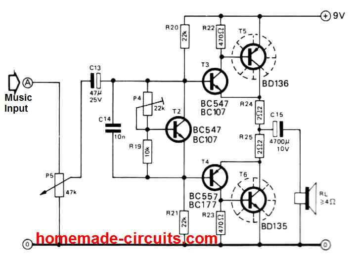
Once connected and powered, the small 5 watt amplifier will be able to boost the output to a much amplified over any 8 ohm 5 watt loudspeakers.
The 47K is used for adjusting the volume output of the amplifier, and the 22K preset is used for setting up the quiscent current of the amplifier.
The 22k preset must be adjusted by connecting a small 100mA lamp in series with the supply line. And the input point A must shorted to ground.
Next, adjust the 22k preset until there no illumination present on the lamp. The quiescent current of this amplifier is not set.
The lamp could be removed now, and the amplifier used normally for the amplifying the input signal.
Mini Audio Booster
The circuit has a standard design where the common emitter input stage (Q1) is directly connected to the common emitter driver stage (Q2), which is then directly coupled to the complementary emitter follower output stage (Q3) (Q3 - Q4).
R7 gives almost 100% negative feedback at DC, allowing the circuit a voltage gain of about unity at DC.
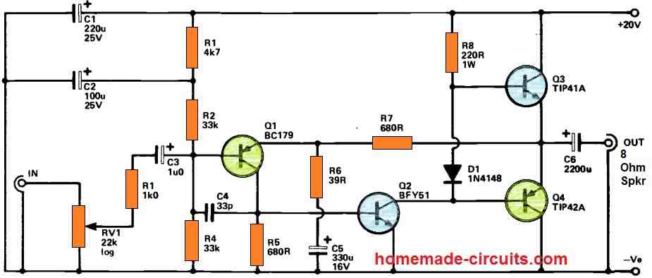
D1 is used to provide a tiny standing bias to the output transistors, which, when combined with the rather significant level of negative feedback, decreases cross-over distortion to an undetectable level.
The emitter follower output stage provides the circuit with a low output impedance, allowing the load to be driven effectively with large output currents. Q4 drives the loudspeaker during positive going output cycles, whereas Q3 drives the speaker during negative going output cycles.
Simple Single Transistor Min Amplifier Circuit
Here is a simple circuit that adds 20 dB of audio amplification. The part numbers displayed offer an accuracy of plus or minus 3.0 dB from 120 to more than 20,000 Hz.
If you want to minimize the circuit's low-end roll-off frequency, replace capacitor C1 to 0.1 uF. The booster may be used as a power amplifier stage in the mini-stereo circuit.
Simple Class AB Amplifier
The schematic for a basic three-transistor is shown next. A supplemental amplifier in class AB capable of driving around 1 Watt into a 3-ohm speaker load. The transistor Q1 is set up as a common-emitter amplifier.
The combination of speaker SPKR1, resistor R1, and potentiometer R5 is used to drive a load. The corresponding emitter-follower stage, consisting of Q2 and Q3, follows and amplifies its output voltage.
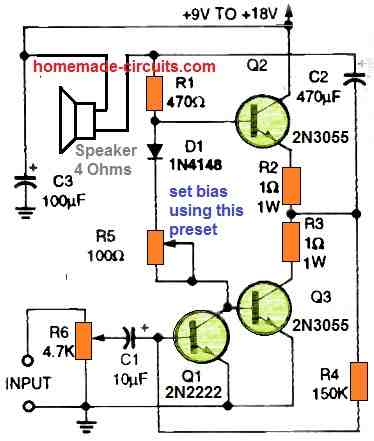
The amplifier's output is delivered to the intersection of SPKR1 and R1 via capacitor C2, providing a low-impedance drive for SPKR1. This bootstraps the R1 at the same time, giving the circuit a high voltage gain.
The output is likewise fed back to Q1's base via R4, resulting in a negative feedback loop which causes a base bias.
Trimmer potentiometer R5 should be cautiously adjusted to reduce audible signal crossover distortion while maintaining the minimum possible quiescent current draw.
Adjust the quiescent current to 10 to 15 milliamperes to get a decent result.
LM380 Amplifier Circuit
This straightforward small amplifier circuit is designed for basic music amplifications application, which is an incredibly valuable device.
The circuit schematic of the simple amplifier is shown below. The circuit is structured around the well-known LM380N IC which includes the benefit over other ICs of needing hardly any discrete parts to accomplish an affordable amplifier.
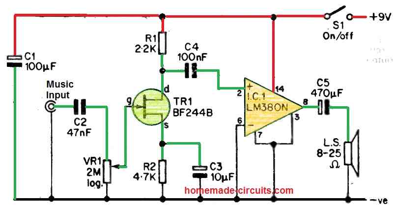
An effective amplifier could be built by using this IC and only about three discrete parts.
They are an output DC blocking capacitor (C5) an input DC blocking capacitor (C4), and a supply decoupling capacitor (C1).
You will find a couple of disadvantages to applying only a fundamental circuit of this type in the current plan, and these are the insufficient voltage gain and input impedance of the design.
The LM380N provides standard input impedance and voltage gain quantities of 150k and 50 correspondingly.
Preferably with this amplifier circuit these must be approximately 10 times larger in each scenario, in order that the amplifier is able to work through high impedance low level loads, say for example a crystal mic.
Therefore, to be able to enhance the input impedance and voltage gain of the fundamental design, an FET common source preamplifier stage has been included.
This FET is denoted by Tr1, VR1 forms the volume control, and this makes the gate bias resistor for Tr1 to times higher.
Capacitor C2 supplies DC blocking on the input. Switch S1 is used as the on/off switch, which could be ganged together with VR1 if required.
Capacitor C1 is the only power decoupling capacitor which is necessary for the complete LM380 mini amplifier circuit.
Simple Amplifier Circuit using BD140 Transistor
This extremely straightforward audio amplifier produces approximately one watt of output power when supplied with 6 volts.
It is designed for use with two speakers, making it a suitable choice for battery-powered devices, especially those accommodating small 50 mm speakers commonly found in transistor radios.
For proper operation, it's advisable to mount the BD140 transistor (Q3) on a small heatsink.
Additionally, adjusting the value of resistor R1 is necessary to achieve a 1.5-volt drop across each speaker.
When connected to 4-ohm speakers, the amplifier delivers its full 1-watt output, while with 8-ohm speakers, it provides half of that output power."

Questions & Answers
thanks dear 🙏
Respected Swagatam,
I would build small AB class amplifier for very low load impedance about 0.5, or 1ohm, or even bellow, with power supply of 3 – 5V. So, I prefer your schematics 1. and 6. Amplifier should be very high quality, and because, I can myself to figure out how to precisely adjust quiescent current, and zero voltage on the output line (half voltage of the power supply if it is not differential). Also, I heard if someone like to drive low impedance speaker, then is favorable to double, triple, or more number of output transistor pairs (o.e, BC547/557). But I can not to figure out what value should be emitter resistors of output transistors, to amplifier be stable and good quality. From what is this dependent? Thanks in advance!
Petar
Thank you Petar,
The circuit #1 shown is a good starting design but for your requirement of 0.5 ohm to 1 ohm load and low voltage, it is not enough in it original form.
Please upgrade the following:
Yes, you need to Add 2 to 3 extra output transistor pairs
Use low emitter resistors (0.1 to 0.22 ohm)
Add a bias trimmer preset in series with R1, to fine-tune quiescent current
Increase power supply to at least 5V to 9V
Use heatsinks and good bypass caps
Once done, you might get a stable, high-quality AB amp that works great even with very low impedance speaker loads.
Thanks!
Very good excellent
Dear Sir, I’m a hobbyist in audio electronics in special.
I would like to build a hi-fi audio power amp. following your schematic with 2N 3055 power transistor and duel symmetrical supply & with differential cascade input. Please let me know if it’s PCB is available, supply voltage & ampere per channel. I love it as it used simple yet vastly available transistors like BC 548/558 or BD 139/140 s .
I’ve made some circuits with 2N 3055 MJ 3055 etc.
Thanks ????
Hi Chayan,
Sorry, I do not have the PCB design for the specified circuit. I would recommend you to first build it over a strip board by soldering…if it works well then you can get a PCB designed for it.
Thank you so much. But I think it to be better to make a PCB done first and then to make and try to run the circuit. I’ve some bitter experiences of huge noises earlier when I made Power and Pre amp./ Tone controls on vero foils due to unwanted oscillation and feedbacks.
I’m hopeful for success as circuit seems to be very well composed.
Regards ????
Show quoted text
OK no problem, you can build the PCB first and then test the circuit on it. All the best to you.
small fm radio build , push button type seek for stations and volume, but why does it have to have 2 seperate 3-5volt feeds, does not work if i use same usb feed for both?, john.
Which schematic are you referring to exactly?
Hi sir swag
Sir i just want to ask you how to make jig test for mini amplifier and for bluetooth speaker. Thanx
Hi Dennis,
In the jig you just need to have a supply DC input, a loudspeaker terminal output and a built in 1 kHz oscillator. Once the amplifier is connected to these inputs it can be quickly tested. I am not too sure about the Bluetooth speaker jig testing.
Ok sir thank you. because the jig test you taught me for tvs ,amplifier,a 100w bulb works very well and shorted issue is easily detected
Thank you Dennis! That’s great, please keep up the good work!
Thanks for your reply.
Good day, I’m very pleased with your topic, though some are not so easy for me to understand by now. I’m basically a hobbist, and I like lot to learn electronics. I would like to learn how to make some changes to amplifier to make them work in lower voltages. If it is possible, we can contact through my email.
Thanks in advance!
Tank you, you can definitely operate any amplifier with lower supply voltages without any changes, but the sound output will proportionately reduce.
Dear Shri Swagatam,
Your ideas are really innovative. I was curious of knowing the location of connection/tap points in the circuit diagram to save/record voice/sound played onto a pendrive and vice cersa for also for a location port/taps connecting it (pendrive/usb drive) to play the saved/recorded music similar to what used to be earlier recoding head in case of cassette player.
Regards
Thank you Dear Mohan Bhagwat ji, appreciate your feedback! However, the circuits explained above are basic audio amplifiers which cannot integrated with any save or record facilities.
The “input” points is the place where small music signals are supposed to be fed, so that they can be amplified on the connected speaker. This input signal could be from a MIC, an old cassette play head, from headphone jack etc
Thank you for your circuits they are very informative and helpful and I look forward to getting then in my email so thank you for your emails.
I would love to see a circuit for a hearing aid type circuit that could be run with one or two earphones and could be run from a lipo battery at 3.7 volts so it could be charged to save cost with batteries and be easy to make and have an acoustic adjustment to cut out background noise so volume is not the highlight just very low distortion and good quality sound with adjustable volume my mother in law would love me to make one!!
Thanks Bob
Thank you, I appreciate your feedback, presently I do not have the hearing aid circuit with the mentioned specs, if I happen to find one, will try to update it here.