In this post I have explained how to use a transistor emitter follower configuration in practical electronic circuits, we study this through a few different example application circuits. An emitter follower is one of the standard transistor configurations which is also referred to as common collector transistor configuration.
Let’s try to first understand what’s an emitter follower transistor and why it’s called a common collector transistor circuit.
What’s an Emitter Follower Transistor
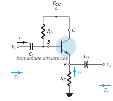
In a BJT configuration when the emitter terminal is used as the output, the network is called an emitter-follower. In this configuration the output voltage is always a shade lower than the input base signal due to the inherent base to emitter drop.
In simple terms, in this type of transistor circuit the emitter seems to be following the base voltage of the transistor such that the output at emitter terminal is always equal to the base voltage minus the forward drop of the base-emitter junction.
We know that normally when the emitter of a transistor (BJT) is connected to the ground rail or the zero supply rail, the base typically requires around 0.6V or 0.7 V to enable complete switching of the device across its collector to emitter. This operational mode of the transistor is called the common emitter mode, and the 0.6V value is termed as forward voltage value of the BJT. In this most popular form of configuration the load is always found connected with the collector terminal of the device.
This also means that as long as the base voltage of the BJT is 0.6V higher than its emitter voltage, the device becomes forward biased or gets turned ON into conduction, or gets optimally saturated.
Now, in an emitter follower transistor configuration as shown below, the load is connected at the emitter side of the transistor, that is between the emitter and the ground rail.
When this happens the emitter is not able to acquire a 0V potential, and the BJT is unable to turn ON with a regular 0.6V.
Suppose a 0.6V is applied to its base, due to the emitter load, the transistor only just begins conducting which is not enough to trigger the load.
As the base voltage is increased from 0.6V to 1.2V, the emitter begins to conduct and allows a 0.6V to reach its emitter, now suppose the base voltage is further increased to 2V….this prompts the emitter
voltage to reach around 1.6V.
From the above scenario we find that the emitter of the tramsistor is always 0.6V behind the base voltage and this gives an impression that the emitter is following the base, and hence the name.
The main features of an emitter follower transistor configuration can be studied as I have explained below:
- The emitter voltage is always around 0.6V lower than the base voltage.
- The emitter voltage can be varied by varying the base voltage accordingly.
- The emitter current is equivalent to the collector current. This
makes the configuration rich in current if the collector is directly
connected with the supply (+) rail. - The load being attached between the emitter and the ground, the base
is attributed with a high impedance feature, meaning the base being not
vulnerable of getting connected to the ground rail through the emitter,
does not require high resistance to safeguard itself, and is normally
protected from high current.
How Emitter Follower Circuit Works
The voltage gain in an emitter follower circuit is approximated to be Av ≅ 1, which is quite good.
In contrast to the collector voltage response, the emitter voltage is in phase with the input base signal Vi. Meaning both input and the output signals tend to replicate their positive and negative peak levels, simultaneously.
As understood earlier, the output Vo appears to be "following" the input signals levels Vi, through an in-phase relationship, and this represents its name emitter follower.
The emitter-follower configuration is mainly used for impedance-matching applications, due to its high impedance characteristics at the input and a low impedance at the output. This appears to be the direct opposite of the classic fixed-bias configuration. The outcome of the circuit is quite similar to as that acquired from a transformer, in which the load is matched to the source impedance for achieving highest levels of power transfer through the network.
re Equivalent Circuit of Emitter Follower
The re equivalent circuit for the above emitter follower diagram is shown below:
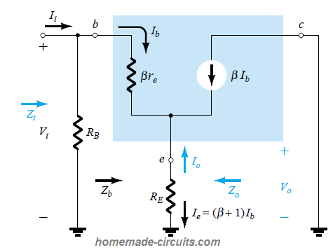
Referring to the re circuit:
Zi: The input impedance can be calculated using the formula:
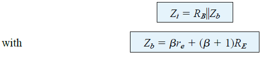
Zo: The output impedance can be best defined by first evaluating the equation for the current Ib:
Ib = Vi / Zb
and subsequently multiplying by (β +1) to get Ie. Here's the result:
Ie = (β +1)Ib = (β +1)Vi / Zb
Substituting for Zb gives:
Ie = (β +1)Vi / βre + (β +1)RE
Ie = Vi / [βre + (β +1)] + RE
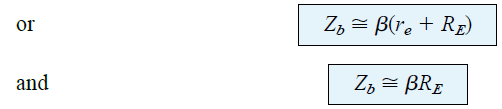
since (β +1) is almost equal to β and βre / β +1 is almost equal to βre / β = re we get:
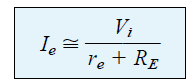
Now, if we build a network using the above derived equation, presents us with the following configuration:
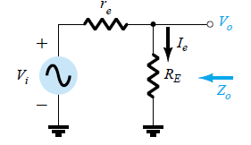
Therefore, the output impedance could be determined by setting the input voltage Vi to zero and
Zo = RE||re
Since, RE is normally much bigger than re, the following approximation is mostly taken into account:
Zo ≅ re
This gives us the expression for the output impedance of an emitter follower circuit.
How to use an Emitter Follower Transistor in a Circuit (Application Circuits)
An emitter follower configuration gives you the advantage of getting an output that becomes controllable at the base of the transistor.
And therefore this can be implemented in various circuit applications demanding a customized voltage controlled design.
The following few example circuits show how typically an emitter follower circuit can be used in circuits:
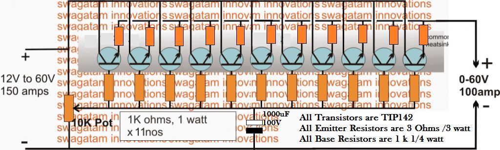
Simple Variable Power Supply:
The following simple high variable power supply exploits the emitter follower characteristic and successfully implements a neat 100V, 100 amp variable power supply which can be built and used by any new hobbyist quickly as a handy little bench power supply unit.
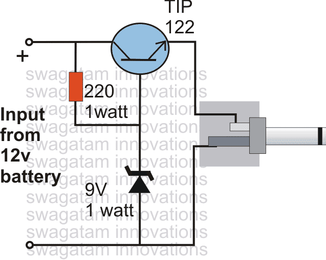
Adjustable Zener Diode:
Normally a zener diode comes with a fixed value which cannot be changed or altered as per a given circuit application need.
The following diagram which is actually a simple cell phone charger circuit is designed using an emitter follower circuit configuration. Here, simply by changing the indicated base zener diode with a 10K pot, the design can be transformed into an effective adjustable zener diode circuit, another cool emitter follower application circuit.
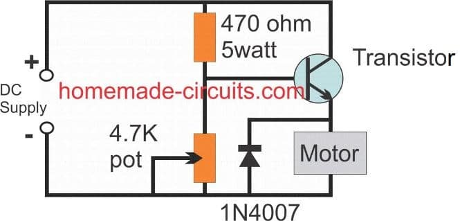
Simple Motor Speed Controller
Connect a brushed motor across the emitter/ground and configure a potentiometer with the base of the transistor, and you have a simple yet very effective 0 to maximum ranged motor speed controller circuit with you. The design can be seen below:
Hi Fi Power Amplifier:
Even wondered how amplifiers are able to replicate a sample music into an amplified version without disturbing the waveform or the content of the music signal? That becomes possible due to the many emitter follower stages involved within an amplifier circuit.
Here’s a simple 100 watt amplifier circuit where the output power devices can be seen configured in an source follower design which is an mosfet equivalent of a BJT emitter follower.
There can be possibly many more such emitter follower application circuits, I have just named the ones which were easily accessible to me from this website, if you have more info on this, please feel free to share through your valuable comments.


Comments
As seen in the Simple Motor Speed Controller could you specify wich trasistor it is being used on the circuit .
The transistor type will depend on the motor current specifications….what is your motor amp rating?
Your transformées AC to DC circuit diagram is interesting. My need is to be able to dim that voltage to run a resistive heater from 0 to 40V when delivering 0 to 15À.
How can you help?
Can you please specify which circuit exactly are you referring to? I will try to help!
in circuit diagram of example of Simple Variable Power Supply
how we calculate value of base resistance and emitter resistance
thanks so much
You can perhaps find all the related calculations in the following article:
https://www.homemade-circuits.com/how-to-design-a-stabilized-bench-power-supply-circuit/
can i use a emitter follower circuit to control a 12v 5 watt heater? or could you please recommend a circuit that could let me control this heater. i tried many kinds of pwm circuits but they dont last. thank you in advance!!
Yes you can but the transistor will heat up when the voltage to the heater is reduced.
Instead you can try a PWM method, which will keep the transistor cooler, as shown in the following example:
Making an Adjustable Electromagnet Circuit
You can replace the EM with your 12v heater. The parallel diode can be removed for your application
I greatly appreciate your fast reponse to my query sir! Your a cool dude…. i will give your advice a try and hope that it wont burn out the mosfet. I will also try to mount my mosfet on a old cpu heat spreader to try and pull more heat away from the mosfet. Again sir i thank you and i wish you success jn life…. more power and GOD BLESS!!!!
Thank you Dexter, I wish you all the best! Let me know if you have any further problems!
When I use 555 timer for slow start pwm there I have face a problem frequency very can you help me how I use it for fix frequency and slow start pwm.
Please show me the link of the schematic that you have used, I’ll try to help!