In this post I have explained a 2 simple, single chip digital potentiometer circuits which can be controlled through a single pushbutton, a dual pushbutton (up/down) or even through external digital (CMOS/TTL) input triggers.
1) About DS1869 Dallastat
TM is a rheostat or potentiometer. This unit delivers 64 conceivable consistent tap outputs over the over-all resistive spectrum.
The typical resistive stretches are 10 kΩ, 50 kΩ, and 100 kΩ. The Dallastat may be governed by both a mechanical switch contact closure input or simply a computerized reference input for example a CPU.
The DS1869 functions from 3V or 5V supplies. Wiper setting is sustained without having power by means of a EEPROM memory cell range.
The EEPROM cell array is going to endure higher than 50,000 writes. The DS1869 can be obtained from two regular IC packages such as an 8-pin 300-mil DIP and an 8-pin 208-mil SOIC.
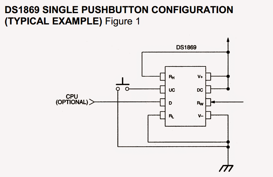
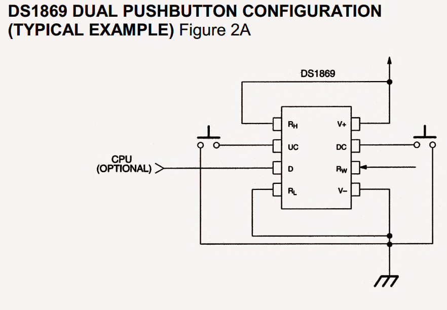
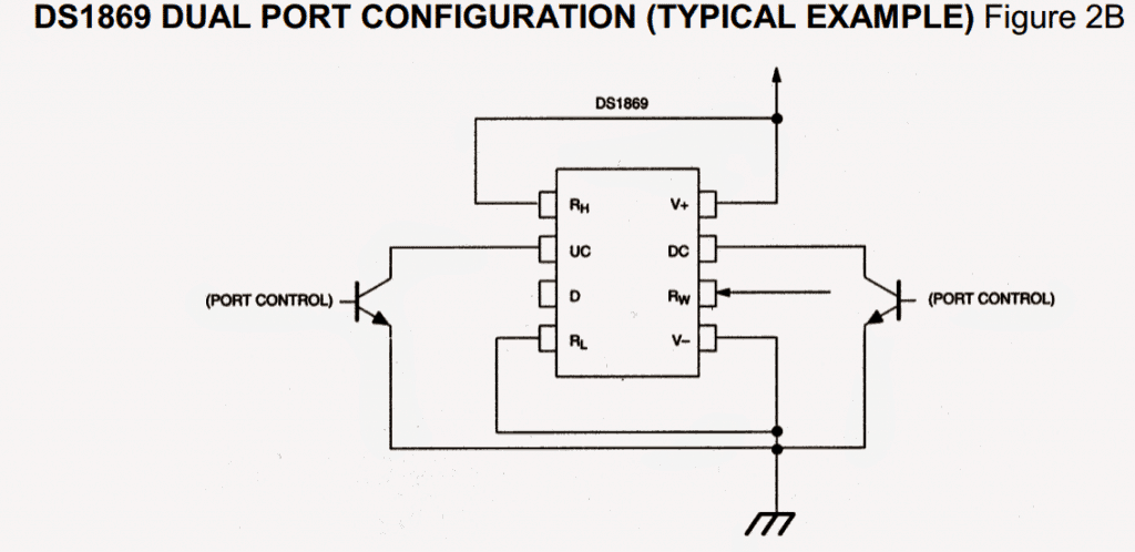
The DS1869 could be set up to function employing an individual pushbutton, combined pushbutton or electronic base input by switching power-on setting.
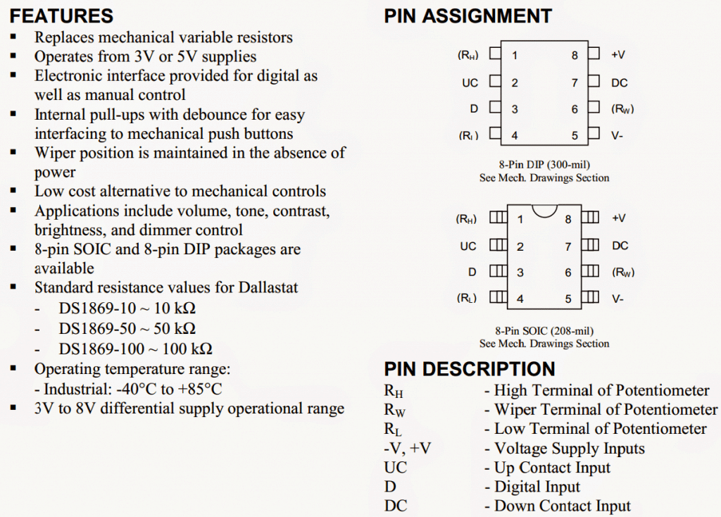
This is drawn out in Figures 1 and 2. The DS1869 pinouts enable entry to each ends of the potentiometer RL, RH, in addition to the wiper, RW.
Control inputs contain the digital reference input, D, the up contact input, UC, and the down contact input, DC. Supplementary pins incorporate the positive, +V, and negative, -V, supply inputs. The DS1869 is stipulated to function from -40°C to +85°C.
Main Features and Pinout Details:
Circuit Operation
The DS1869 could be custom made to execute from an individual contact closure, twin contact closure, or a digital root input. Figures 1 and 2 depict the two contact closure variations.
Contact closure is considered as a changeover from an increased level to a reduced degree on the up contact (UC) or down contact (DC) inputs.
All three control inputs are busy while in a low status and are sedentary while in a high disposition. The DS1869 interprets input pulse widths as the method of regulating wiper motion.
One pulse input on the UC, DC, or D input terminals will result in the wiper placement to relocate 1/64th of the entire resistance.
A changeover from a high to low on these inputs is regarded as the outset of pulse process or contact closure. One pulse has to be more than 1 ms nevertheless running not anymore than 1 second. Pulse timings are presented in Figure 5.
Recurring pulsed inputs may be used to approach via every resistive placement of the unit in a typically rapid technique (see Figure 5b).
The necessity for frequent pulsed inputs is because pulses needs to be split up by optimum time of 1 ms. In the event that the input is not permitted to be sedentary (high) for a minimum of 1 ms, the DS1869 will probably read repetitive pulses as just one pulse.
Pulse inputs continuing more than 1 second will result in the wiper to relocate one place every 100 ms following the preliminary 1-second store time.
The complete time to transcend the whole potentiometer employing a nonstop input pulse is presented the equation below:
≈1 second + 63 X 100 ms = 7.3 (seconds)
Schematic Diagrams
2) Digital Potentiometer using IC X9315
In this second design we investigate the IC X9315 which is actually a solid state digital potentiometer and could be used exactly like a mechanical potentiometer, but through logical supply inputs.
The IC X9315 from Intersil, is a digitally controlled solid state potentiometer, which internally possesses an array of resistors, wiper switches, a controlling system, and a non-volatile memory section.
Block Diagram
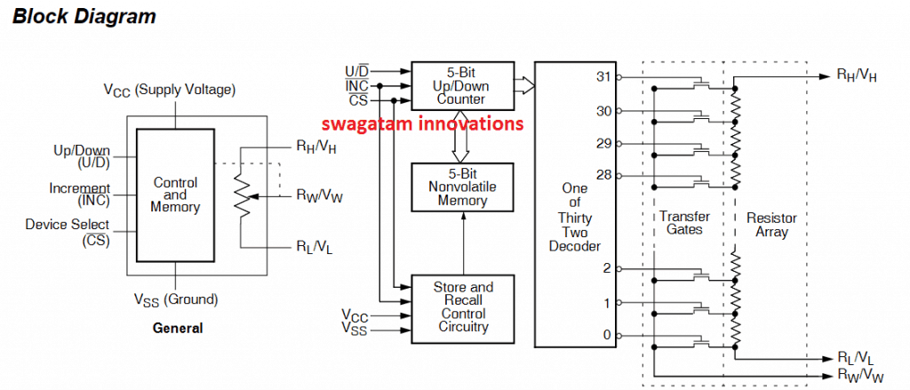
The IC utilizes a 3 wire interface for controlling the various positions of the wiper, and the potentiometer function is implemented through the array of resistors which are 31 numbers of resistive network, associated with the wiper switching network.
The entire array along with the end points of this resistive network are all integrated with the wiper network such that the wiper is able to access any point of the resistor array for executing the corresponding values of the potentiometer output through the 3 wire interface.
The CS, U/D and the INC pinouts of the IC actually control the wiper positioning.
The device can be also used as a 2 terminal potentiometer or a 2 terminal variable resistor.
The system becomes enabled and selected as soon as the CS input is applied a LOW logic (0V).
The value of the instantaneous wiper position is saved in non-volatile memory space, whenever the CS pinout is
delivered with a HIGH logic, in conjunction with INC input.
As soon as the store function is finished the X9315 is put into a low power standby position, until the unit gets selected yet again with a logic LOW.
How the IC X9315 digital pot works
You will find 3 parts in the X9315: the input control, counter and decode sections; the non-volatile memory; and the resistor range.
The input control segment works very much like an up/down counter. The output of this counter is processed and translated to activate a solitary electronic switch integrating a stage from the resistor range with the wiper terminal.
During appropriate and necessary circumstances the details of the counter is often saved in non-volatile memory and held on to for long term usage.
The resistor range is made up of 31 unique resistors attached in a sequence. At both terminate of the range and in between every resistor there exists an electronic switch which interlinks the network at that position with the wiper.
The wiper, during its course across specified end points, works similar to its mechanical counterpart and doesn't shift further than the final location.
That means, the counter will not flip over, if its clocked to either of the extreme end positions. The electronic switches within the product work in a “make before break” kind of setting once the wiper begins changing tap placements.
When the wiper is transferred a few positions, multiple taps tend to get coupled to the wiper for t IW (INC to V W change). The R TOTAL figure for the product may momentarily be minimized with a considerable magnitude when the wiper goes through a number of positions.
Once the unit is switched OFF, the instantaneous wiper position is saved and preserved in the non-volatile memory.
Next time the power is switched ON, the saved data from the memory are usually remembered and the wiper is placed to the position which was on the last stored power OFF.
How to Program The digital Pot IC
The INC , U/D and CS inputs manage the movements of the wiper together with the resistor array. With CS fixed LOW the unit is selected and activated to react to the U/D and INC inputs. HIGH to LOW transitions on INC goes through a a five bit incrementing or decrementing counter sequence (based upon on the state of the U/D input) .
The output from this counter is decoded back to pick one out of thirty two wiper placements together with the resistive array. The position of the counter is saved in non-volatile memory, anytime CS changes HIGH and also when INC input is HIGH.
As soon as the wiper action is carried out as explained previously and once the newest placement is arrived at, the device must maintain INC LOW whilst putting CS at a HIGH. The fresh wiper placement is now preserved as long as it's not altered by the circuit, or a power OFF is not enforced.
Otherwise the system may select the X9315, activate the wiper shifting, and subsequently unselect the unit without saving the newest wiper placement in non-volatile memory.
The above feature makes sure that the IC always switches ON with the last wiper position data from its memory.
Pin Description of the Device
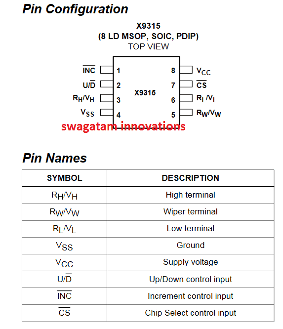
The (RH /VH ) and (RL /VL ) terminals of the X9315 could be compared to the fixed terminals of any standard mechanical pot.
Vcc/Vss:
The Vcc pin is the + DC for the IC, while the Vss is the (-) supply pin of the IC
The minimum voltage is Vss and the maximum is Vcc.
RL /VL and RH /VH and U/D
The terms RL /VL and RH /VH refer to the relative positions of the potentiometer with respect to the wiper transitional path as selected by the U/D input, and not the voltage level on the terminal.
RW /VW RW /VW
RW /VW RW /VW indicate the wiper link and could be compared with any standard mechanical pot.
A given position of the wiper across the resistor array is determined by the control inputs.
The terminal resistance of the wiper is typically around 200 Ω when the supply at Vcc = 5V.
Up/Down (U/D )
The signal on U/D pinout controls the direction of the wiper movement and determines the incrementing or decrementing situation of the counter.
Increment (INC )
The INC input wil respond to a negative-edge trigger. Whenever INC is switched the wiper moves and causes the counter to increment or decrement in the direction which will depend on U/D input logic level.
Chip Select (CS )
The potentiometer system becomes enabled and selected as soon as a low logic is applied at the CS pinout of the IC. The instantaneous value of the pot position gets stored in the nonvolatile memory of the chip, as soon as a high logic is detected at the INC pin of the chip. Once this happens the IC goes into low power sleep mode, until the CS pin is selected again with a logic low.
Courtesy: https://www.intersil.com/content/dam/Intersil/documents/x931/x9315.pdf

Comments
Can the digital pot’s wiper and resistive elements work with audio signal that is biased at mid supply rail, such as in 9V single supply guitar effect pedals? I have the impression that it can’t, because the chip is 5V, but I could be wrong, because perhaps the 5V is just for its internal digital circuitry that is controlling the wiper?
Yes, I too think it can’t, because the IC works with 5V and your input is based on 9V…a 5V will not block 9V efficiently, so it might fail to work.
Hi,
Is there an alternative to the DS1869 digital pot chip?
Local suppliers are out of stock or have discontinued supply of the DS1869.
Thanks
Mike
Hi,
You can try searching “digital pot IC datasheet”, you might come across many alternatives.
Hi all,
I saw this page because I would to simulate an PT100/1000 sensor using digital pot IC.
I want to use that on a resistive divider to set R.eq from 80 to 200 ohm.
Tipicaly the input voltage of PT100/1000 sensor is by 2,5 to 5Vdc. Is this usable for this application? Thank you
Yes you can use it…
Hi Swagatam,
I’m still trying to get schematics but in the meantime could you help me with a circuit to use the DS1869 in the two switch configuration as a stereo volume control. Will I need two DS1869, one for each channel? I’m struggling to workout where the audio signal will come in unless this would be VCC and the output on the wiper pin? Maybe this chip is not the most suitable for the application I need? Any suggestions would be appreciated.
Hi John,
the audio signal can e applied to the RW pin, via a capacitor. After this the UC, Dc pins could be used for th required UP/Down conrol via respective series push-buttons
Many thanks Swagatam, I have sketched out a circuit using two DS1869 ICs to achieve stereo voice activated volume control here:-
However I am not sure where the attenuated audio out would be taken. I would have thought this would be on the wiper pin RW but you state this should be the audio in? Please can you confirm. Also what sort of capacitor would a 10uF electrolytic be sufficient and which way round polarity wise. Also I read on another site that two Digipots don’t necessarily work well together and there may be a dual channel version of the chip that might be better.
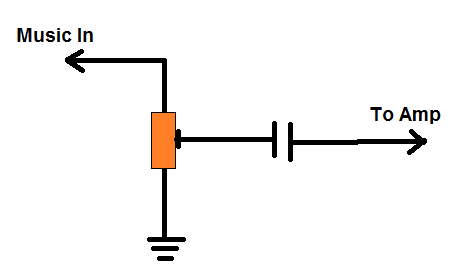
The RH is the music input
RL is the ground
RW goes to the amplifier via a capacitor
Looks OK to me!
In manual version we connect a pot in the following manner:
So now you can easily figure out how to interpret the same in the electronic version
Any capacitor between 1uF and 10uF will work OK
Sorry not sure about the performance, only a practical test will confirm that!
I think there’s some confusion, as per the manual version, the electronic set up is not correct….I will check it out soon
Hi Swagatam,
I came across your post when searching for a DigiPot volume control circuit. I want to control the signal input into four different class D amplifiers connected to speakers in each room. I would like to do this using Amazon Alexa voice control. I had thought about using a two channel Tuya Smart relay.
To substitute for the Up and Down switches. Do you think this would work?
I don’t want to get into PWM and an arduino or similar.
Hi John,
that may be possible, but I will have to see how the switches are wired and their location in the circuit, only then I will able to confirm the application….
Thanks for reply Swagatam I am trying to find the manufacturer of these relay board so I can ask for a schematic, but that’s turning out to be difficult. In the meantime is there a way to send you some screenshots and specifications?
No problem John, you can upload your pictures to any online image hosting site, and provide the link to me….if I it is possible I’ll try to solve it for you!
Hello, I’m looking for something like the Digital Potentiometer IC X9315
that a 3 wire hall effect sensor can be used as the input.
24v dc motor using china motor controller that has a 100k ohm pot for speed control. I want to replace the 100k pot with a digital pot that I can wire in the hall sensor as the speed controller.
Thanks
E
Hello, you can use the concept for your application.
Every single high clock at INC will cause the pot to move up or down….it will move up if the U/D is held high, it will move down if the U/D is held low.
But I am not sure how a hall effect can be used for this….may be the hall effect output will need to be converted to PWM and then applied at U/D…..
Thanks for the quick reply. My hopes is to find a chip like the X9315 that has an analog input.
E