A blocking oscillator is one of the simplest form of oscillators which is able to produce self sustaining oscillations through the use of just a few passive and a single active component.
The name "blocking" is applied due to fact that the switching of the main device in the form of a BJT is blocked (cut-of) more often than it's allowed to conduct during the course of the oscillations, and hence the name blocking oscillator.
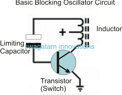
Where a Blocking Oscillator is Typically Used
This oscillator will generate a square wave output which can be effectively applied for making SMPS circuits or any similar switching circuits, but cannot be used for operating sensitive electronic equipment.
The tone notes generated with this oscillator become perfectly suitable for alarms, morse code practice devices, wireless battery chargers etc. The circuit also becomes applicable as strobe light in cameras, which can be often seen just before clicking the flash, this feature helps in reducing the infamous red eye effect.
Due to its simple configuration, this oscillator circuit is widely used in experimental kits, and the students find it much easier and interesting to grasp it details quickly.
How a Blocking Oscillator Works
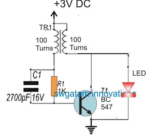
For making a blocking oscillator, the selection of the components become quite critical so that it is able to work with optimal effects.
The concept of a blocking oscillator is actually very flexible, and the outcome from it can be extensively varied, simply by varying the characteristics of the involved components such as the resistors, the transformer.
The transformer here specifically becomes a crucial part and the output waveform heavily depends on the type or the make of this transformer. For example when a pulse transformer is used in a blocking oscillator circuit, the waveform attains the shape of rectangular waves consisting of rapid rise and fall periods.
The oscillating output from this design become effectively compatible with lamps, loudspeakers, and even relays.
A single resistor can be seen controlling the frequency of a blocking oscillator, and therefore if this resistor is replaced with a pot, the frequency becomes manually variable and can be tweaked as per the users requirement.
However care should be taken not to reduce the value below a specified limit which could otherwise damage the transistor and create unusually unstable output waveform characteristics. It is always recommended to position a safe minimum value fixed resistor in series with the pot to prevent this situation.
Circuit operation
The circuit works with the help of positive feedbacks across the transformer by associating two switching time periods viz, the time Tclosed when the switch or the transistor is closed, and the time Topen when the transistor is open (not conducting). The following abbreviations are used in the analysis:
- t, time, one of the variables
- Tclosed: instant at the end of the closed cycle, initialization of the open cycle. Also a magnitude of the time duration when the switch is closed.
- Topen: instant at the every end of the open cycle, or the beginning of closed cycle. Same as T=0. Also a magnitude of the time duration whenever the switch is open.
- Vb, supply voltage e.g. Vbattery
- Vp, voltage within the primary winding. An ideal switching transistor will allow a supply voltage Vb across the primary, therefore in an ideal situation Vp will be = Vb.
- Vs, voltage across the secondary winding
- Vz, fixed load voltage resulting due to for e.g. by the opposite voltage of a Zener diode or the forward voltage of a connected (LED).
- Im, magnetizing current across the primary
- Ipeak,m, highest or the "peak" magnetizing current on the primary side of the trafo. Takes place just before Topen.
- Np, the number of primary turns
- Ns, the number of secondary turns
- N, the ratio of winding also defined as Ns/Np, . For an perfectly configured transformer working with ideal conditions, we have Is = Ip/N, Vs = N×Vp.
- Lp, primary self-inductance, a value calculated by the number of primary turns Np squared, and an "inductance factor" AL. Self-inductance is frequently expressed with the formula Lp = AL×Np2×10−9 henries.
- R, combined switch (transistor) and the primary resistance
- Up, energy accumulated within the flux of the magnetic field across the windings, as expressed by the magnetizing current Im.
Operation during Tclosed (time when the switch is closed)
The moment the switching transistor activates or triggers it applies the source voltage Vb over the transformer primary winding.
The action generates a magnetizing current Im on the transformer as Im = Vprimary×t/Lp;
where t (time) may be a changing with time and initiates at 0. The specified magnetizing current Im now "rides upon" any reverse generated secondary current Is which may happen to induce into the load on the secondary winding (for instance into the control terminal (base) of the switch (transistor) and subsequently reverted to secondary current in primary = Is/N).
This altering current at the primary in turn generates an altering magnetic flux within the transformer's windings; which enables quite a stabilized voltage Vs = N×Vb across the secondary winding.
In many of the configurations the secondary side voltage Vs may add up with the supply voltage Vb; due to the fact that the voltage on the primary side is approximately Vb, Vs = (N+1)×Vb while the switch (transistor) is in the conducting mode.
Thus, the switching procedure may have the tendency to acquire a portion of its control voltage or current directly from Vb while the remaining through Vs.
This implies that the switch-control voltage or the current would be "in phase"
However in a situation of an absence of a primary resistance and negligible resistance on the transistor switching, might result in a rise in the magnetizing current Im with a "linear ramp" which may be expressed by the formula as given first paragraph.
Conversely suppose there is a significant magnitude of primary resistance for the transistor or both (combined resistance R, e.g. primary-coil resistance along with a resistor attached with the emitter, FET channel resistance), then the Lp/R time constant could result in a rising magnetizing current curve with consistently dropping slope.
In both the scenarios the magnetizing current Im will have a commanding effect through the combined primary and the transistor current Ip.
This also implies that if a limiting resistor is not included the effect could increase infinitely.
However, as studied above during the first case (low resistance), the transistor might ultimately fail to handle the excess current, or simply put, its resistance might tend to rise to an extent where the voltage drop across the device might become equal to the supply voltage; causing complete saturation of the device (which may be evaluated from a transistor's gain hfe or "beta" specs).
In the second situation (e.g. inclusion of a significant primary and/or emitter resistance) the (dropping) slope of the current might reach a point where the induced voltage over the secondary winding is simply not sufficient to keep the transistor in the conducting position.
In the third scenario, the core used for the transformer might reach the saturation point and collapse which int turn would stop it from supporting any further magnetization, and prohibit the primary to secondary induction process.
Thus, we can conclude that during all the three situations as discussed above, the rate at which the primary current rises or the rate of rise of the flux in the core of the trafo in the third case, might show a dropping tendency towards zero.
Having said this, in the first two scenarios, we find that despite of the fact the primary current seems to continue its supply, its value touches a constant level which might be just equal to the supply value given by Vb divided by the sum of the resistances R at the primary side.
In such a "current-limited" condition the transformer's flux might tend to show a steady state. Except the changing flux, which might keep inducing voltage across the secondary side of the trafo, this implies that a steady flux is indicative towards a failure of induction process across the winding resulting in the secondary voltage dropping to zero. This causes the switch (transistor) to open.
The above comprehensive explanation clearly explains how a blocking oscillator works and how this highly versatile and flexible oscillator circuit may be used for any specified application and fine tuned to the desired level, as the user may prefer to implement.

Comments
Hello. Is it possible to synchronize this oscillator with an external pulse, similar to CRT TVs? If so, where should such pulses be applied? To the transistor base? Best regards!
Hi, I don’t think this circuit can be synchronized with an external pulse, because this circuit is self-oscillatory and cannot be synchronized with any external frequency.
Greetings: I need a circuit (on / off) that shuts off in 10 minutes and after locking it disconnects the battery from the car and continues to block the ignition …
Hello, it can be easily, but how would you start the car again after the timer locks the ignition?
Good Day sir,
Im initially try to applied blocking oscillator scheme combined with inverter to make some adjustable multy DC voltage input, and multy AC voltage output, is it possible that way? please share your idea beacuse im still confused looking for a right scheme
Hi Miftah, sorry I could not understand what exactly you are trying to implement and in what manner…please explain it a bit more elaborately
Hi sir, is it possible to build multyrange DC voltage input inverter circuit and also adjustable its inverted voltage signal using blocking oscillator topology, that somehow it seems able to generate constant output when it used for LED even with small DC voltage source,
sorry if I made you confused 😀
Hi Miftah, I have no idea how a blocking oscillator could be used to build a multirange power inverter circuit, if you have any ideas please let us know, I’ll be happy to share it here.
Neat Post
Hi Swagatam,
I’ve seen that people often suggest you some project. I’ve not found where I can do that in this site. Can you tell me? thx.
Hi Michael, readers usually explain the required concept through comment or through emails. If I find the request feasible for me and useful for my website, I design and publish it for the readers.
Hii swagatam i want to build my own 9 chanel remote for plane operation plz helpe
Hi Munim, making a 9 channel remote control could be quite complex, instead you can easily buy one readymade from the market.
thank you for your replay I need an advice about my project which I have completed few months ago the project is free energy perfectly working with 150 percent efficiency means if i have 1 volt 1amp i can make 1.5 volts 1.5 amps after dichargeing 1volt 1 amp from battery or capacitor i can charge it fully and i will have 50 percent energy to use now the problem is how to make it commercial to power the world iam very scared to tell anyone i don't know any big people iam from a small village with 7th class educational qualification iam 20 years old i have started this project when i was fifteen it took me 5 years to develop fully working circuit and it is my own concept i can explain its theory and build a small machine in one day with this concept we can built a power plant easily but how to find an investor
OK that looks interesting, you should a make a video of the working of the design and post it on Youtube.
Iam connecting a battery to my circuit through an ammeter in series battery voltage 12 volts 7.5 amps current drawn from my battery is 12 volts 1 amp the output connected to load through ammeter series measuring 1.5amps and a volt meter in parallel 18 volts output
Patenting can be quite expensive, around 50k to 1 lakh INR…so it's not useful initially, you don't need to tell the entire concept just tell me the results in detail, and how you are measuring it.
You can also make a prototype and create a Youtube video of its working.
additionally, you can submit an article to my website discussing the results only, I'll publish it.
if it really works then investors will automatically approach you.
is it good to register a patent before telling any one
the circuit iam using is not over unity it is only 75 percent efficient another 75 is from nature as you said over unity Is not possible I know we cannot move 2 electrons with 1 electron
my concept is simple the secondary of my transformer wont produce eddy current
somasunder, what concept have you applied please provide the rough details, I am sure what you are getting is not over-unity, so please don't be so excited so soon, I do not wish to disappoint you, but you will discover the bitter truth sooner or later and that could make you sad…
but somehow If you succeed then you could approach Mr. Narendra Modi he will surely help you, but before that make sure your concept is really working….
yes, the joule thief principle looks quite identical to this, which has the hallmark feature of squeezing out last drop of charge left in a battery.
thanks for the interesting updates! appreciate it.
hi sir my name is sunder first I like to thank you for your great work I have a dought if I connect 1kv inverter to a 12v 180 amps battery without any load how long will it take to discharge the battery fully I hope you will replay to me because it is really important to my life
Thank you Somasunder, you can use the following software to roughly determine the back up time of a given battery…although you are not using any load, there has to to some current consumption by the inverter itself which will need to be specified for the calculation
https://www.homemade-circuits.com/p/battery-calculator.html