In this post I have explained about MOSFET bidirectional power switches, which can be used for operating a load across two points bidirectionally. This is simply done by connecting two N-channel, or P-channel MOSFETs back to back in series with the specified voltage line.
What is a Bidirectional Switch
A bidirectional power switch (BPS) is an active device built using MOSFETs or IGBTs, which allows a two way bidirectional flow of current when powered ON, and blocks a bidirectional flow of voltage when powered OFF.
Since it is able to conduct across both ways, a bidirectional switch can be compared and symbolized as a normal ON/OFF switch as shown below:

Here, we can see a positive voltage is applied at point "A" of the switch and a negative potential is applied at point "B", which allows the current to flow across "A" to "B". The action can be reversed by simply changing the voltage polarity. Meaning, the points "A" and "B" of the BPS can be used as interchangeable input/output terminals.
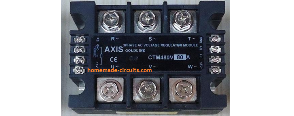
The best application example of a BPS can be seen in all MOSFET based commercial SSR designs.
Characteristics
In Power Electronics, the characteristics of a bidirectional switch (BPS) is defined as a four-quadrant switch having the ability to conduct positive or negative current in the ON-state, and also block positive or negative current in OFF-state. The four-quadrant ON/OFF diagram for a BPS is shown below.
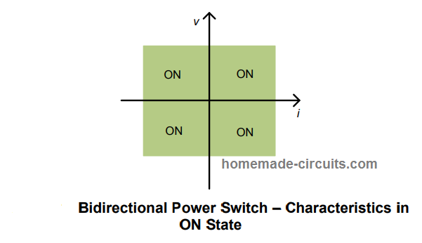
In the above diagram, the quadrants are indicated in green color which indicates the ON state of the devices regardless of the polarity of the supply current or the waveform.
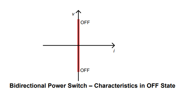
In the above diagram, the red straight line indicates that the BPS devices are in OFF state and offers absolutely no conduction regardless of the polarity of the voltage or the waveform.
Main Features a BPS Should Have
- A bidirectional switch device must be highly adaptable to enable easy and quick power conduction from both sides, that is across A to B and B to A.
- When used in DC application, a BPS must exhibit minimum on state resistance (Ron) for improved voltage regulation of the load.
- A BPS system must be equipped with proper protection circuitry to withstand sudden in rush current during a polarity change, or at relatively high ambient temperature conditions.
Bidirectional Switch Construction
A bidirectional switch is constructed by connecting MOSFETs or IGBTs back to back in series as shown in the following figures.
Here, we can witness three fundamental methods through which a bidirectional switch can be configured.

In the first diagram, two P-channel MOSFETs are configured with their sources connected back to back with each other.
In the second diagram, two N-channel MOSFETS can be seen connected across their sources for implementing a BPS design.
In the third configuration, two N-channel MOSFETs are shown attached drain to drain for executing the intended bidirectional conduction.
Simulation
Basic Functioning Details
Let's take the example of the second configuration, in which the MOSFETs are joined with their sources back to back, let's imagine positive voltage is applied from "A", and negative to "B", as shown below:
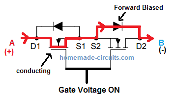
In this case we can see that when the gate voltage is applied, current from "A" is allowed to flow through left MOSFET, then through the internal forward biased diode D2 of the right side MOSFET, and finally the conduction completes at point "B".
When the voltage polarity is reversed from "B" to "A" the MOSFETs and their internal diodes flip their positions as shown in the following illustration:
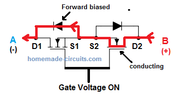
In the above situation, the right side MOSFET of the BPS switches ON along with D1 which is the internal body diode of the left side MOSFET, to enable the conduction from "B" to "A".
Making Discrete Bidirectional Switches
Now I have explained how a bidirectional switch can be built using discrete components for an intended two way switching application.
The following diagram shows the basic BPS implementation using P-channel MOSFETs:
Using P-Channel MOSFETS
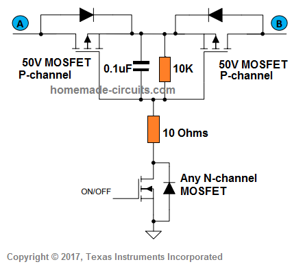
When point "A" is positive, the left side body diode gets forward biased and conducts, followed by the right side p-MOSFET, to complete the conduction at point "B".
When point "B" is positive, the opposite side respective components become active for the conduction.
The lower N-channel MOSFET is controls the ON/OFF states of the BPS device through appropriate ON/OFF gate commands.
The resistor and the capacitor protect the BPS devices from a possible in rush current surge.
However, using P-channel MOSFET is never the ideal way of implementing a BPS due to their high RDSon. Therefore these might require bigger and costlier devices to compensate against heat and other related inefficiencies, compared to N-channel based BPS design.
Using N-Channel MOSFETS
In the next design we see an ideal way of implementing a BPS circuit using N-channel MOSFETs.
In this discrete bidirectional switch circuit, back-to-back connected N-chanel MOSFETs are used. This method demands an external driver circuit for facilitating the two way power conduction from A to B and in reverse.
The Schottky diodes BA159 are used to multiplex the supplies from A and B to activate the charge pump circuit, so that the charge pump is able to generate the necessary amount turn ON voltage for the N-channel MOSFETs.
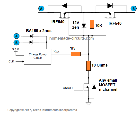
The charge pump could be built using a standard voltage doubler circuit or a small boost switching circuit.
The 3.3 V is applied for powering the charge pump optimally, while the Schottky diodes derive the gate voltage directly from the respective input (A/B) even if the input supply is as low as 6 V. This 6 V is then doubled by the charge ump for the MOSFET gates.
The lower N-channel MOSFET is for controlling the ON/OFF switching of the bidirectional switch as per desired specifications.
The only disadvantage of using an N-channel MOSFET compared to the previously discussed P-channel are these extra components that may consume extra space on the PCB. However, this disadvantage is outweighed by the low R(on) of the MOSFETs and highly efficient conduction, and low cost small sized MOSFETs.
That said, this design also does not provide any effective protection against over heating, and therefore oversized devices may be considered for high power applications.
Conclusion
A bidirectional switch can be quite easily built using a couple back to back connected MOSFETs. These switches can be implemented for many different applications which require a bidirectional switching of the load, such from AC source.
References:
TPS2595xx, 2.7 V to 18 V, 4-A, 34-mΩ eFuse With Fast Overvoltage Protection Data Sheet


Comments
Very helpful – I’m building a voltage data logger. I need to switch in/out a couple of resistors to adjust the attenuation of a voltage divider to produce +/-5V from an arbitrary voltage into an ADC (via a precision rectifier). This just solved my switch problem.
And over the years I’ve found many helpful ideas from your posts 🙂
Thank you for your good work.
Thank you, and glad you found the post helpful! Let me know if you have any further problems!
I have a relay circuit where the contacts have to be isolated from the coil drive circuit, including the ground. I am switching three different DC power sources at once with 13 mechanical relays 400 times per second and have to keep both sides of the supplies isolated. I like the idea of MOSFETS as switches but haven’t figured out how to keep the gate supply grounds isolated from the source grounds. Any thoughts?
You can probably try the last concept explained in the following article for solving the query:
https://www.homemade-circuits.com/solid-state-relay-ssr-circuit-using-mosfets/
great website for both beginner and professional. one question: if we have a stove and dryer but our electric line is not enough for them to work same time. can you suggest a circuit or component that will cut the stove from power when dryer is working, and vice versa?? in other words allow only one of the two appliances to work at any time ?? by the way they both use 3phase power. thanks.
Thank you for liking this website, you can simply do it with a relay, that will enable you a manual change over from one load to the other…
Hi Swagatam,
Thanks for this information already! Just one quick question. Is this setup ensuring a SOA (safe operating area) for the FET’s? If not, how can we accomplish this?
We’re facing quite large inrush-currents and need protection for that.
Hi Mart, SOA depends on your selection of the MOSFETs. If you ensure that the SOA of the devices are appropriately rated as per the input out specifications of the circuit, then all will be fine….
Will the body diodes in the MOSFET’s cause a voltage drop in both directions?
negligible voltage drops….
hi Swagatam,
how to calculate the switching loss of the the mosfets in the common source configuration im using the common source n channel mosfet configuration in my AC load dimmer circuit.
im not able to find any document how to calculate the switching loses.
please let me know your comments
Hi Shubham, switching losses will be through dissipation, RDSon of the MOSFET and the internal diode’s forward voltage drop specifications….these can be calculated by standard formulas.
Hi Swagatam,
im switching the MOSFETS by PWM signal, and the ON and OFF time is not Fixed, so im considering the DC at 25%, 50%, 75% and 100% with the frequency of 1Khz. im using the combination as above using n channel MOSFET with High side driving
so if i consider the standard formula like this it will not applicable for my design.
Psw-H = 1/2 X Vin X Io X (tr +tf) X fsw
please correct me if im wrong.
please let me know your comments.
Thanks,
Shubham.
Hi Shubham, the above explained bidirectional switch does not incorporate high side or low side mosfet as in H-bridge, so I think the mentioned formula might not be relevant for this concept.
Don’t worry about it, I have official permission from ti.com to refer their concepts with a link back. ti.com allows bloggers to promote their datasheets, and applications with appropriate references.
I hope that answers your question.
This is true; however, you did not include the application note used in your references, nor did you include a source on every image you lifted. In fact, you did the opposite – adding your own watermark implies that you created the images, which you did not. Even edited, you have to give credit to the actual source. Otherwise, that’s plagiarism, friend.
You can argue as much as you want, but all those are baseless. May be you do not know the exact purpose of a water mark it is to ensure that the images do not get copied by other sites without a credit. I have added my watermark in the middle of the image so that copying from here becomes impossible for other sites.
Better read the entire screenshot attached in the previous comment.
Hello Sawagatam,
Thanks for the reply. We will try and update the same.
Hello Swagatam,
Greetings…!
We are using Bi-directional N Channel Mosfet with Common Source config. We are using these in buck converter circuit. The issue we are facing is the left side N-channel Mosfet gets heated more when current in it increases to 15A DC. Let me know if any details you need further from my side.
Hello Rachit, did you try operating the device normally like a simple bidirectional switch for a 15 amp load? Please try it normally without a buck converter, if it works without issues then the problem could be the buck converter circuit and the involved inductor specs.
Hi Swagatam,
With regard to your silicon bidirectional switch, your ‘conduction path’ diagrams are really useful to understand what is going on. I do however have a comment: a turned-on FET will conduct in reverse through the FET itself, and when switched off it will only conduct through the body diode. When switched on (as it would be when it’s twin is turned on), the preference will usually be through the FET as its’ resistance will present a far lower voltage drop than the body diode will. So your diagrams should show that.
Also, there is no diagram for P-channel common-drain (although the N-channel has common-drain and common-source). I have not seen one of this configuration anywhere else either. Is there a reason for this? Would it work?
Thanks Owen, The body diode is connected in reverse to the drain/source polarity of the FET, so if the FET is conducting would mean the body diode is reverse biased, so it can never conduct. P-channel MOSFET would also work using a slightly different configuration, however the P channels are seldom preferred as switches due to their high RDSon and inefficient response to high currents.
Thanks for the reply.
What I was angling at was the FET that is conducting via the body diode (FET2 in the current flow diagram immediately under ‘Basic Functioning Details’). FET2 (being turned on at the same time as FET1) would have a milli-ohm resistance. From what I’ve read, a FET channel can conduct in both directions and if that is the case, the voltage drop across the channel would be lower than the voltage drop across the body diode. Much the same as the way I understand a syncronous rectifier works.
(sorry, I haven’t dealt much with FETs so I am only going on “internet information”)
Hence, when the “silicon bidirectional switch” is “on”, it appears to be a milli-ohm resistor rather than appearing to be a diode in series with a milli-ohm resistor?
Sorry I have not yet investigated this aspect of a MOSFET. If that is the case then what is need of the “protection” body diode, since the MOSFET would easily bypass the reverse current also? In my opinion, when a positive is applied across gate/source, current cannot flow from source to drain.
True sir swagatam, please investigate that aspect and let us know. Am really following
During direct conduction (both MOSFETs ON) the current does NOT flow through the body diode. Otherwise, you would get a 0.6 – 0.9 V drop between in and out!
that drop is negligible and acceptable. Current will always take the easier course, that is though the forward biased diode.