In this post I have explained the main specifications and pinout functions of the IC CS209A along with other technical aspecst of the chip.
Introduction
The device CS209A is a bipolar monolithic IC specifically designed for metal detecting circuit applications. The IC fundamentally has a built-in oscillator stage, a couple of current regulator stages, a low level feed back circuit, and a few other relevant stages like peak detection/demodulation stage, a comparator stage and a couple of complementary output blocks.
How IC CS209A is Designed to Work
An external LC tank circuit becomes imperative while applying the IC in a metal detector configuration. The externally connected LC circuit in association with the in built oscillator circuit initiates the required oscillations in the circuit in a controlled manner.
The amplitude of the oscillations largely depends on the Q factor of the connected LC tank network.
When the LC network responds with a low Q levels, the adjustable low level feedback circuit enables drive for sustaining the oscillations.
The peak demodulator stage detects the falling section of the oscillator package and feeds a demodulated waveform to the comparator stage as input information.
The comparator initiates and set up the complementary outputs by comparing the received information from the demodulator stage with an internal reference level.
The main features of the IC include the following:
- Separate current regulator stage for the oscillator,
- Negative transient blocking,
- Adjustable low level feedback,
- Enhanced temperature compensation,
- Minimal current consumption = 6 mA @ 12V DC,
- Output current sinking feature = 20mA @ 4 V DC, and 100 mA @ 24 V DC.
- The absolute maximum rating of the chip are given below:
- Supply voltage not to exceed 24 V DC.
- Maximum allowable power dissipation is 200 mW,
- Maximum temperature limits at which the chip needs to be stored should not cross -55 and +165 degree Celsius.
- Junction temperature must be maintained within -40 and +150 degree Ce;cius.
- Electrostatic discharge should never cross the potential of 2 kV, except the tank pin out.
- While soldering the chip, the maximum contact time of 10 seconds is permissible @ 260 degree Celsius for each individual pins of the IC.
Electrical Characteristics of the IC
- Some of the important electrical characteristic of the IC CS209A as observed for a given set of tests may be understood with the following points:
- Supply current consumed b the IC was noted as 3.5 to 6 mA @ 4 volts, 6 to 12 mA at 12 volts and 11 to 20 mA @ 24 volts.
- For the tank circuit, the current consumption was noted as -300 to -100 uA @ 20 volts.
- Demodulator charge current was noted to be in between -30 to -10 uA @ 20 volts.
- Output leakage current was witnessed to be 0.01 to 10 uA @ the maximum volts of 24.
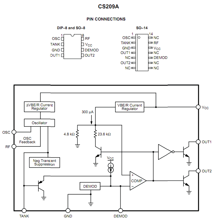
Pinout Functions
The pin-outs of the IC may be understood with the following description:
- Pin #1 is denoted as OSC, when connected with a feedback resistor between this pin and the RF, configures the detection range of the chip.
- Pin #2 is assigned as the TANK pin out and is responsible for connecting the parallel tank network.
- Pin #3 is the ground input of the IC.
- Pin #4 and the pin #5 are the complementary outputs of the IC denoted as OUT1 and OUT2 respectively.
- OUT1 shows a open collector output in response to a “LOW”, that is when a metal presence is sensed.
- OUT2 shows an opposite response with the above conditions.
- Pin #6 (for DIP-8 and SO-8) and pin #10 (SO-14) which are denoted as DEMOD, is the input pin out to the comparator responsible for controlling the pair of complementary outputs.
- Pin #7 (for DIP-8 and SO-8) and pin #12 (SO-14) is the supply voltage input.
- Pin #8 (for DIP-8 and SO-8) and pin #13 (SO-14), assigned as RF is associated with the adjustable feedback resistor which is connected between the OSC and the RF.
- Remaining pin outs are all NC (not connected).

Questions & Answers
Hello dear professor, I would like to request you to send me a complete schematic diagram using two 555 ICs to build a pulse metal detector. Thank you.
Hi Mohammad, I will try to design it soon and let you know…