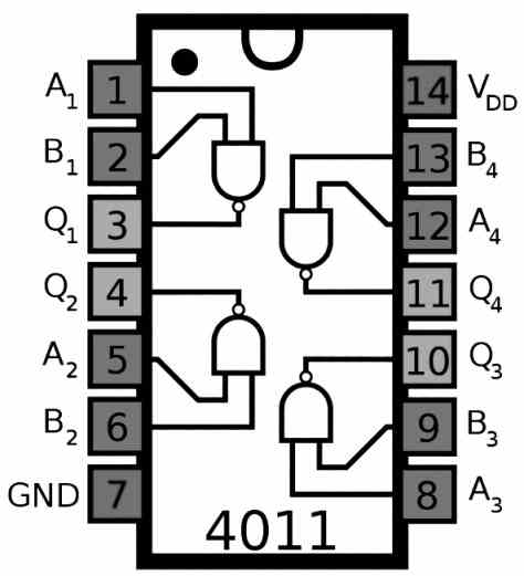
The IC 4011 is a quad 2-input NAND gate integrated circuit. It is widely used in digital electronics applications for logic gate functions. Here is a typical datasheet for the IC 4011:
General Specifications:
- Supply voltage: 3 to 15V DC
- Input voltage: 0 to VDD
- Output voltage: 0 to VDD
- Operating temperature: -55°C to 125°C
- Current consumption: 8mA (max)
- Output current: 6mA (max)
- Propagation delay: 60ns (typ) at VDD=10V, RL=1000 Ohm
Pin Configuration:
The pinout configuration of the IC 4011 can be viewed in the following diagram:

Features:
- Four independent NAND gates in one IC
- High noise immunity
- High-speed operation
- Low power consumption
- TTL and CMOS compatible
- Buffered outputs
- Pin compatible with other 4000 series logic gates
Applications:
- Logic gate functions
- Data processing
- Clock generation
- Memory addressing
- Control circuits
For more applications circuit you can read the following artilce:
Note: This datasheet is for general reference only, as specific features and specifications may vary depending on the manufacturer and version of the IC. It is important to consult the datasheet for the specific IC being used in any given application.


Need Help? Please Leave a Comment! We value your input—Kindly keep it relevant to the above topic!