In this post I will talk about 5 outstanding, easy to build, low distortion Hi-Fi 40 watt amplifier circuits that can be further upgraded to higher wattage through some minor tweaks.
This article was contributed to me through email by a dedicated follower
Although you may find several hybrid output modules available, hardly any of these are able to blend simplicity with affordability along with great overall performance.
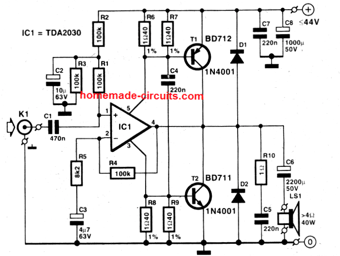
One of them is SGS's chip TDA2030 employed in the present amplifier. The layout of the amplifier is uncomplicated: a power opamp accompanied by two bridge tied output transistors. The audio signal is given to the non-inverting input of power opamp lC1 through socket K1 and capacitor C1.
The supply current to the IC oscillates according to the input signal.
Due to this, it exhibits equally changing voltage drop around resistors R6, R7. R8, and R9 given that these are in the source lines to the opamp. So long as the current is below 1 A, the voltage drop over the resistors is going to be inadequate to turn on transistors T1 and T2. Which means outputs up to 2 W into 4 Ohm speakers are supplied totally by the opamp.
As soon as the output current gets higher than a level of 1 A, the transistors are switched on and reinforce the power output of the amplifier.
If the input signal is low results in insufficient quiescent current through the transistor, however since this happens through the opamp crossover network, issues are eventually evaded.
The IC additionally delivers thermal compensation, and therefore ensures guaranteed stability of the operating point.
The supply voltage might range between 12 V and an absolute maximum of 44 V. Building of the amplifier on the PCB must be easy.
The transistors along with the IC should be installed and insulated on to a heat sink of approximately 2 k W-1. Apply lots of heat conducting composite. The supply line needs to be guarded by a 3.15 A fuse. line should be protected by a 3.15 A fuse.
Circuit Diagram
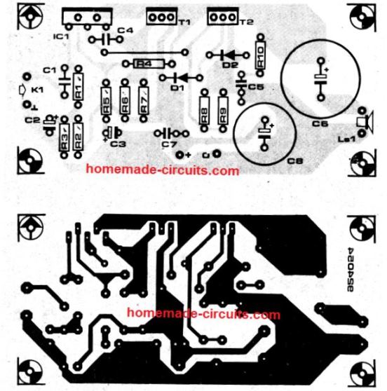
PCB Design
Parts List
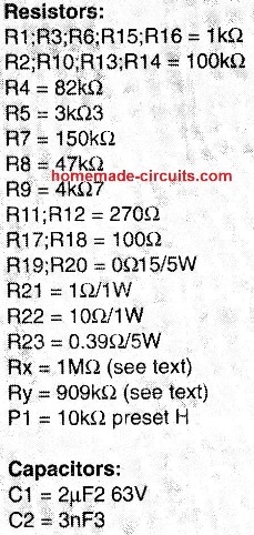
Resistors, all 1/4 watt 5% unless specified
- R1 to R4 = 100K
- R5 = 8k2
- R6 to R9 = 1. 4 ohm 1%
- R10 = 1 ohm
Capacitors
- C1 = 470 nF
- C2 = 10uF, 63V radial
- C3 = 4.7uF, 63V radial
- C4, C5, C7 = 220 nF MKT or Ceramic
- C6 = 2200uF, 50V radial
Semiconductors
- D1, D2 = 1N4007
- T1 = BD712
- T2 = BD711
- IC1 = TDA2030
Miscellaneous
- K1 = Audio socket, or jack
- Heatsink = 2K W^-1
- Insulating washers etc for IC1, T1, T2
Technical Specifications
Operating Voltage: 44V Maximum
Output Power = 22 watt in 8 Ohm Speaker and 40 watts in 4 Ohm speaker with THD = 0.1%
Harmonic Distortion Chart
- 1 kHz in 8 ohm at 11 watt = 0.012%
- 1 kHz in 4 ohm at 20 watt = 0.032%
- 20 kHz in 8 ohm at 11 watt = 0.074%
- 1 kHz in 8 ohm at 1 watt = 0.038%
- 1 kHz in 4 ohm at 1 watt = 0.044%
- Quiscent Current = 38mA approximately
- Efficiency = 8 Ohm 62.5%
- Maximum Load = 4 Ohm 64%
2) 40 Watt Amplifier using IC LM391
This second design is a powerful, no-frills medium power amplifier that may be specifically matched to use in ‘combo‘ type of portable amplifiers which are popular with guitarists and jazz music artists.
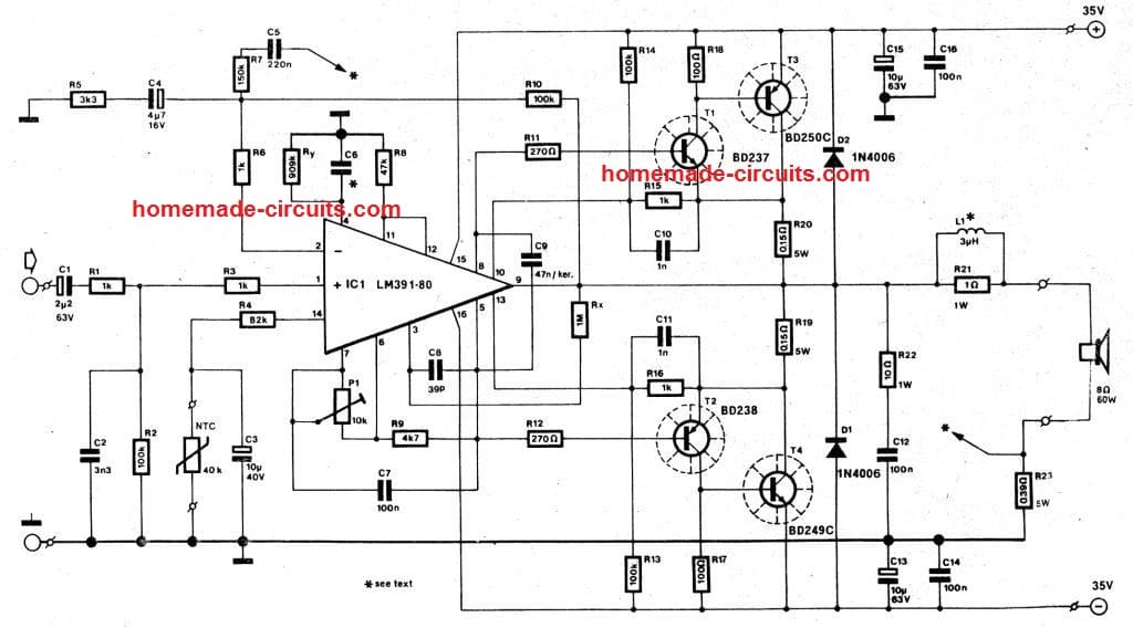
The amplifier is an efficient blend of a built-in audio driver IC the LM391-80, and a push-pull power output stage built with bipolar transistors.
A few unique aspects of the design are reviewed below.
The NTC, which is in physical contact with the power output transistors, allows the LM391 to shut off the power stage when this overheats. The starting point of this heat safety is situated at an NTC current of about 200 pA.
The electrolytic capacitor grounding the NTC acts to present a ‘soft start',which is, to avoid a noisy click on or other befuddling noise from the loudspeaker when the amplifier is toggled on.
It might seem that the protection is way too sensitive, and therefore some trial and error for the value of R4 or that of the NTC, might be required. It is easy to apply feedback in the amplifier by connecting R23 to line network C5-R7.
The other components, along with R10 decide the frequency response of the amplifier which might require fine-tuning to fulfill specific demands. The component numbers I have I have explained in this article may, nonetheless be okay for the majority of applications.
The result of experimenting with different values of C5 and R7 is easy to determine (or hear) by shorting out R23 briefly. For 4 Ohm loudspeakers, R23 needs to be reduced to 0.18 Ohm. Sadly, the LM391-80 is vulnerable to oscillation, which must be kept under control through components RX, C6, C8 and C9 (in many instances, C6 could be removed).
Resistor RX specifically minimizes the open-loop gain. If RX is employed, Ry has to be attached to compensate the resulting off-set voltage. Components R22 and C12 constitute a Boucherot network which functions to stabilize the amplifier at high frequencies. The input of the amplifier must be operated by a low-impedance source which is able to deliver ‘line’ level audio signals (0 dB].
Network R1-C1 attenuates amplitudes above 50 kHz or so. The quiescent current of the amplifier is defined by preset P1. Adjust this control to 0 Ohm in the beginning, and fine tune it right up until a quiescent current of 50 mA is established.
You can increase this to 400 mA should you be looking for low distortion. The power transistors are all positioned at the same section of the PCB in order that they could be clamped onto a common heatsink, along with the NTC.
The heat sink needs to be pretty large with a thermal resistance of 1 K Wsl or lesser. Observe that L1 is made of 20 turns of 0.8 mm dia. enameled copper wire wound around R21. C9 is a ceramic capacitor.
Circuit Diagram
Technical Data
Now let's check out, a few tested data:
With supply voltage: 35 V; R23 short-circuited:
3-dB bandwidth (8 Q]: approx. 11 Hz to 20 kHz
THD (transient harmonic-distortion) at 1 kHz: . 1 W into 8 Ohm: 0.006% (Iq = 400mA) 1 W into 8 Ohm: 0.02% (Iq = 50 mA) 65 W into 8 Ohm: 0.02% (Um = 873 mV) 80 W into 4 Ohm: 0.2% (Um = 700 mV; onset level of current limit).
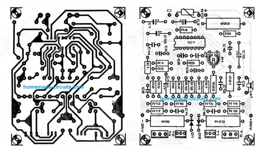
PCB and Component Layout
Parts List
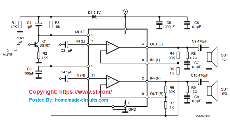
3) 40 watt Power Amplifier using IC LM2876 from Texas Instruments
The third design is yet another cool Hi-Fi 40 watt power amplifier circuit which utilizes a single chip LM2876 for delivering the specified amount of music power over a 8 ohm speaker.
The IC LM2876 is a high-grade audio amplifier chip which is designed to continuously handle 40 watts of average power over an 8 Ohm loudspeaker with a THD of 0.1%, and a frequency range of 20 Hz to 20 kHz.
The performance of this IC is far better than other hybrid ICs due to its built in feature called Self Peak Instantaneous Temperature control circuitry, or the SPiKe.
The "SPiKe" includes a complete protection of the chip against output over-voltage, under-voltage, overload and accidental short circuits.
The IC LM2876 exhibits excellent signal-to-noise ratio above 95 dB, guaranteeing excellent Hi-Fi level sound clarity and reproduction.
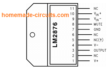
Pinout Diagram of LM2876
Circuit Diagram
The complete circuit diagram of this LM2876 based 40 watt amplifier is presented below:
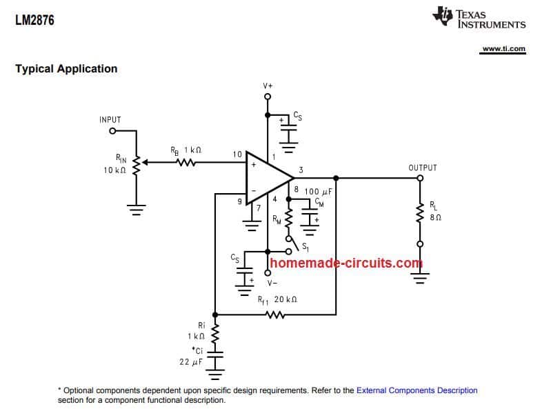
For more info on this please visit the datasheet of the IC
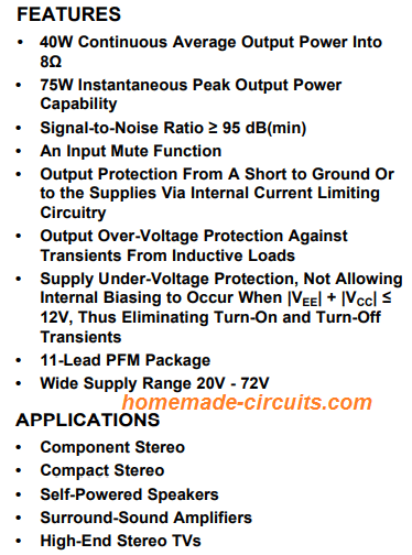
4) 40 watt Stereo Amplifier Circuit using IC TDA7292
So far we have discussed amplifiers with mono 40 watt output, however this fourth circuit in the list is designed to offer a stereo 40 + 40 watt output through a single chip IC TDA7292. So if you are looking for a stereo version of 40 watt amplifier then this design will fulfill your requirement very easily.
This outstanding single chip stereo amplifier is manufactured by ST microelectronics.
The circuit requires hardly any components and could quickly configured using a well deigned PCB which is furnished in the datasheet irself.
Main Features
- Wide supply voltage range (from +/-12 V ± 33 V)
- Works with dual supply for optimal output power
- Designed to deliver full output power 40 W + 40 W into 8 Ω with supply voltage = ±26 V and Total Harmonic Distortion not more than = 10%
- Internally eliminated “pop” sound when power is turned on/off
- Feature a Mute option which is also (“pop”-free)
- When the Mute pin is grounded, the IC goes into a low consumption Standby more.
- Internally the IC is Short-circuit protected, meaning th IC will not burn or get damaged when output is accidentally short circuited or over loaded.
- Also, the IC features an in-built Thermal overload protection, so overheating will also not damage the IC.
Complete Circuit Diagram
Absolute Maximum Rating
The following are the maximum absolute rating of the IC TDA7292, that should not be exceeded to safeguard the IC from getting permanently damaged:
- DC supply voltage ±35 V
- (IO) Output peak current (internally limited) 5 A
- (Ptot) Power dissipation Tcase = 70°C 40 W
- (Top) Operating temperature -20 to 85 °C
- (Tj) Junction temperature -40 to 150 °C
- (Tstg) Storage temperature -40 to 150 °C
Reference: For more details and the complete PCB design, you can refer to the original datasheet of the IC.
5) 40 Watt Amplifier with only Transistors
All the designs explained above are dependent of integrated circuits, and we all know how easily these ICs can get obsolete at any point of time. Perhaps the best way to have a universal evergreen amplifier design is to have it in the form of discrete transistorized version, as shown in this fifth final design:
This is actually the shortened version of the popular 100 watt amplifier from this website. It has been simplified by removing a couple of mosfets and reducing the supply input to 24V.
The parts indicated in the above transistorized 40 watt amplifier circuit looks a little unconventional and might not be readily available in the market. However, the beauty of such transistorized versions is that the active components can be easily substituted with equivalent values. For this design also we can find the appropriate equivalents and replace them here for getting the same flawless results.
The amplifier is superbly designed by the Hitachi engineers for delivering outstanding clarity with minimum distortions. I have tested it and was quite thrilled with its huge adjustable power range and exceptional output quality.
For the entire parts list please visit this article.

Comments
What is the value of “CS” capacitors
Positive and Negative legs?
It is just a filter capacitor. You can try any value between 100uF and 1000uF.
Hi Swagatam;
I had bought a circuits when I was not interested in electronic. There are main parts as TDA2030, 50K Pot, some diodes, capacitors and resistors and also 3 couples of pitch screw pin socket for input and output connection each couple has 2 pins. One of them is for 12 V DC input. Other one is assigned for the HP. And third one is set for entrance. (entrance written on it) I have checked this entrance socket pins, one is short contact with the DC 12 V ground and other pin is short contact with the one pin of the HP input. I think that this circuit cannot be connected with the PC USB output. since there is no input on the circuit from the usb data output. If the datum is enough to comment on it please I need your commentary. Best Regards (P.S.: My aim is to use this circuit from usb instead of my broken embedded pc sound car)
Hello sir, how were you? It’s been a long time. I have a problem with the diagram at the top of tda7292. I see +Vs but no _Vs on the diagram.
Sincerely
Thank you Daouda, I am good!
There’s no (-) in the amplifier, there is a (+) and 0V, the 0V or GND line is at the bottom of the circuit.
Merci beaucoup monsieur
You are welcome Daouda!
Hi Suat,
the audio input pin of any amplifier can never be connected with the positive supply line, that looks impossibles. You must check it again. You can see in the TDA2030 circuit diagram given in the above article. The audio input is protected with C1, and it is not connected with the positive DC line directly.
Also I did not understand what HP stands for?
excuse me Swagatam, please let me tidy up;
there are 3 pitch screws; 1- 12 V DC input no problem 2- HP stands for (hoparlor) speaker no problem and 3- Other pitch screw (entrance written) which also has 2 pins and one pin is connected to ground and other pin is connected to one pin of the speaker output pitch screw. Kind Regards
Thank you Suat,
Yes I understand, but the audio input pin has to go through a capacitor and then to the IC inputs. So the audio input which comes from a capacitor goes to the data pin of the USB, the 5V of the USB should be left unconnected. 12V should be supplied separately to the amplifier, and the ground pin of the amplifier should be connected with the ground pin of the USB
Hi Swagatam;
As far as I understand that is important not to damage the main board. So please let me confirm and understand exactly. We have the USB output at one side and other side we have TDA2030 circuit. Supposedly USB has 4 pins output; 2 are assigned for voltage and others are for data transfer. I will only connect the ground to 12 V input of the TDA2030. The other 2 pins of TDA2030 are assigned for the speaker that is clear and no problem. And the remaining are 2 data pins from USB and 2 input pins of TDA2030 called as entrance so USB 2 data pins will be connected to entrance pins. Best Regards
Hi Suat,
Here’s what exactly you need to do!
1) +5V from USB = Do not connect anything keep it unconnected.
2) Ground line from USB = Connect it with the ground line of the TDA2030 amplifier.
3) USB data pins = Try connecting one of these pins with the audio input pin of the TDA2030 amplifier. But I am not sure whether the data pins output audio frequency or digital frequency?? If its digital frequency then the amplifier may not work
4) TDA2030 Amplifier Vcc = Connect it with an external +12V power supply
5) TDA2030 Amplifier Ground = Connect it with the ground of the external power supply
Thanks for this article. I am needing an amp and finding that all the lower cost retail stuff is class D which I do not want. I forgot about the “all in one” amplifiers on a chip. I found a F8-24 transformer (24v 4 amp) on digikey along with the LM2876. I think a pair of F8-24s for my + and – supply will work good which should give me about a +-30v supply.
I’m a just retired BSEE who did software my whole career so I’m sick of software. Had electronics as my hobby in the 1980s, so maybe it can become my hobby again.
Thanks for your feedback, though class D amplifiers are rated highly efficient in terms of cost and consumption, analogue amplifiers are known for their high quality distortion free music…..there are many analogue designs in this website also which you can try experimenting with…
Hi sir, if I want to built the “40 Watt Amplifier with only Transistors” which is a modified design from the 100w
amplifier, can I use two 1N4148 diodes to replace the 1k VR and avoid to set the current. I ask because it was done on the 100w model and I wonder if this will work on the modified 40w model as well.
Hi Rafael, yes you can try by referring to position of the diodes as shown in the last diagram of the following article:
https://www.homemade-circuits.com/how-to-make-simplest-100-watt-mosfet/
Sir, I went through your articles on audio pre-amplifier circuits. Can you please provide a stereo preamplifier circuit with good gain along with tone control facility and also with a facility to add microphone inputs with provision for connecting a usb board so that mp3 music can be played from a pendrive. If you can add a mixer circuit also then I will be able to play the instrumental music from pendrive and my children can sing through the microphone. Also I will be able to listen mp3 music when my children are not practicing. I am a middle class family member and so cannot afford costly audio equipment. If you can provide the above circuit, that will be beneficial for lot of people. Thank you sir.
Hi Sabu, you can try the simple concepts presented in the following article:
https://www.homemade-circuits.com/4-channel-dj-audio-mixer-circuit-part-1/
If possible I may update more such designs, having more facilities and enhancements….
Dear Sir,
I had made an amplifier using tda 8946j ic 2 channel 30 watt . Working fine. I have a doubt about calculating the pot in input, also how can i get a subwoofer output from it?
Aju, no calculations are required for the volume control pot. If the supply is below 50 V you can use a 10 k pot efficiently. For subwoofer conversion you will have to employ a low pass filter with the amplifier
good day sir… please sir i made an audio amplifier using tda 2030, dual supply… it was not loud, sir can i add power transistors to increase the out put
You can try replacing the transistors with Darlington type power transistors, such TIP142, TIP147 and see the response!
I am a mother and this helped me!
Glad it helped!!
Sir, part list for TDA2030 need to be corrected i.e C4, C5, C7 = 2200uF, 50V radial schematic read C4, C5, C7 = 220nf
Thank you Onesimus, I have corrected the error as per your suggestions.