The circuits presented in the following article could be used for generating strobed lighting effect over 4 Xenon tubes in a sequential manner.
The proposed sequential xenon lighting effect could be applied in discotheques, in DJ parties, in cars or vehicles, as warning indicators, or as decorating ornamental lights during festivals.
A wide range of xenon tubes are available in the market with a matching ignition transformer set (that we are going to talk about afterwards). In theory, just about any xenon tube works extremely well in the strobe control circuit presented in figure below.
How Xenon Tube Rating is Calculated
The circuit is designed for a '60 Watts per second' xenon tube and this is all it is going to accommodate. Sadly, the power ratings of xenon tubes are typically mentioned as "x" watts per second, which often signifies an issue!
The reason behind the particular capacitor values in the diagram and DC voltage level may be comprehended through the following simple equation:
E = 1/2 C.U2
The quantity of electrical power utilized by the xenon tube may be determined simply by multiplying energy and the xenon repetition pulse frequency.
With a frequency of 20 Hz and a power of 60 Ws, the tube might 'consume' around 1.2 kW! But that looks huge, and can't be justified. Actually, the mathematics in the above is using an incorrect formula.
As an alternative, this should be depending on the optimum acceptable tube dissipation and the resulting energy with respect to the frequency.
Considering that the xenon tube specifications which we are enthusiastic about should be capable of handling a highest possible dissipation up to 10 W, or an optimum level of 0.5 Ws energy should be discharged at 20 Hz.
Calculating the Discharge Capacitors
The above explained criteria calls for a discharge capacitance with a value 11uF and having an anode voltage of 300 V. As could be witnessed, this value matches relatively well with the values of C1 and C2 as indicated in the diagram.
Now the question is, just how do we select the correct capacitor values, in a situation where we have no rating printed on the xenon tube? Currently since we have with us the relationship between 'Ws' and W', the below shown rule-of -thumb equation could be tested out:
C1 = C2 = X . Ws / 6 [uF]
This is actually just a relevant clue. In case the xenon tube is specified with an optimal working range of under 250 continuous hours, it is best to apply the equation over a reduced allowable dissipation. A useful recommendation you may want to follow with regards to all types of xenon tubes.
Ensure that their connection polarity is proper, this means that, attach the cathodes to ground. In many instances, the anode is marked with a red-colored spot. The grid network is either available as like a wire at the cathode terminal side or simply as a third 'lead' between the anode and the cathode.
How Xenon Tube is Ignited
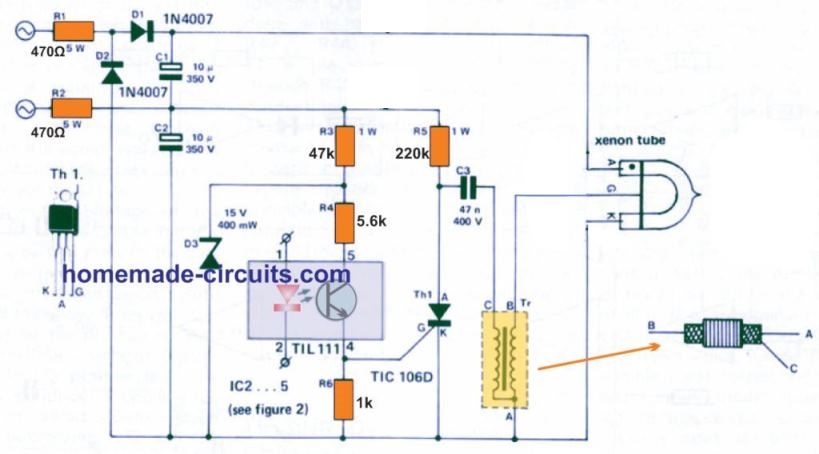
Alright, so inert gases have the ability to generate illumination when electrified. But this fails to clarify just how the xenon tube is actually ignited. The electrical power storage capacitor described previously is indicated in figure 1 above, through a couple of capacitors C1 and C2.
Given that the xenon tube needs a voltage of 600 V across the anode and the cathode, diodes D1 and D2 constitute a voltage doubler network in conjunction with the electrolytic capacitors C1 and C2.
How the Circuit Works
The a pair of capacitors are consistently charged to the maximum AC voltage value and as a result R1 and R2 are incorporated to restrict the current during the xenon tube's ignition period. If R1, R2 were not included the xenon tube would at some point degrade and stop working.
The resistor R1 and R2 values are selected to ensure C1 and C2 are charged up to the peak voltage level (2 x 220 V RMS) with the maximum xenon repetition frequency.
The elements R5, Th1 , C3 and Tr represent the ignition circuit for the xenon tube. Capacitor C3 discharges through the ignition coil's primary winding which generates a grid voltage of many kilovolts across the secondary winding, for igniting the xenon tube.
This is how the xenon tube fires and illuminates brightly, which also implies that now it instantly draws the entire electrical power held inside C1 and C2, and dissipates the same by means of a dazzling flash of light.
Capacitors C1, C2 and C3 subsequently recharges so that the charge allows the tube to go for a new pulse of flash.
The ignition circuit obtains the switching signal through an opto-coupler, an built-in LED and a photo transistor enclosed collectively inside a single plastic DIL package.
This guarantees excellent electrical isolation across the strobe lights and the electronic control circuit. As soon as the photo transistor is lit up by the LED, it becomes conductive and actuates the SCR.
The input supply for the opto-coupler is taken from the 300V ignition voltage from across C2. It is nonetheless lowered to 15V by diode R3 and D3 for apparent factors.
Control Circuit
Since the working theory of the driver circuit is understood, we can now learn how the xenon tube could be designed to produce a sequential strobing effect.
A control circuit for producing this effect is demonstrated in figure 2 below.

The highest repeat strobe rate is limited to 20 Hz. The circuit has the capacity to handle 4 strobe devices at the same time and essentially is made up of range of switching devices and a clock generator.
The 2N2646 unijunction transistor UJT works like a pulse generator. The network associated with this is intended to enable the frequency of the output signal to be tweaked around the 8 … 180 Hz rate using P1. The oscillator signal is fed to the clock signal input of the decimal counter IC1.
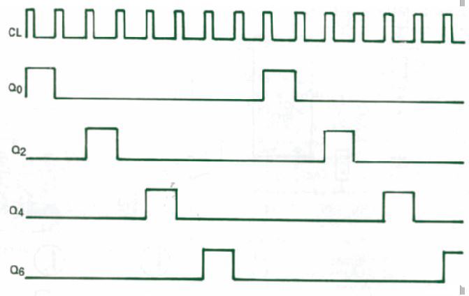
Figure 3 below shows a picture of the signal waveforms at the IC1 output with regards to the clock signal.
The signals coming from the IC 4017 switch at a frequency of 1 … 20 Hz are applied to the switches S1 … S4. The positioning of the switches decides the sequential pattern of the strobe. It allows the lighting sequence to be adjusted from right to left, or the opposite, etc.
When S1 to S4 are set at totally clockwise, the push-buttons become in the operational mode, enabling one of the 4 xenon tubes to be activated manually.
The control signals activate the LED driver stages through transistors T2 . . . T5. The LEDs D1 … D4 work like functional indicators for the strobe lights. The control circuit could be tested by just grounding the cathodes of D1 … D4. These will show immediately whether or not the circuit is working correctly.
A Simple Stroboscope using IC 555
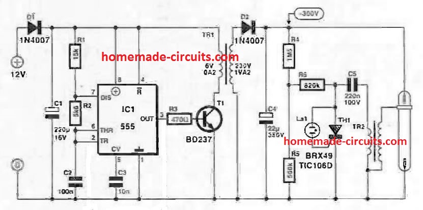
In this simple stroboscope circuit the IC 555 works like an astable oscillator driving a transistor and an attached transformer.
The transformer converts 6V DC into 220 V low current AC for the stroboscope stage.
The 220 V is further converted to a high voltage peak 300 V with the help of the diode capacitor rectifier.
When the capacitor C4 charges up to the triggering threshold of the SCR gate neon bulb, through the resistive network, the SCR fires and triggers the driver grid coil of the stroboscope lamp.
This action dumps the entire 300 V into the stroboscope bulb illuminating it brightly, until the C4 is fully discharged for the next cycle to repeat.
Another Xenon Strobe Light Circuit
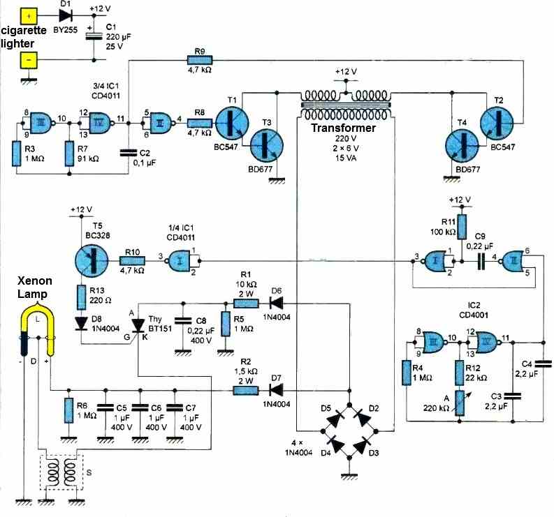
The next setup we propose is a warning strobe light circuit which, in case of a breakdown that immobilizes your vehicle on the side of the road, should be placed to attract the attention of other road users and therefore protect you.
It should be placed on the ground or, even better, on the roof of the vehicle, and will emit regular flashes of light visible from a relatively long distance. It will be directly powered by the vehicle battery by simply plugging it into the cigarette lighter socket, for example.
Power supply
The energy is taken from the vehicle battery through diode D1, which also serves as a polarity detector (Figure 4). Capacitor C1 provides some filtering due to the pulsed operation mode of the circuit. The current consumed can reach several amperes, so it is important to use a suitable power supply wire to limit the voltage drop along the line.
High voltage production
NAND gates III and IV of IC1 constitute an astable oscillator that generates square-shaped pulses on its output with a period of about 20 milliseconds, which corresponds to a frequency of 50 Hz. The output of NAND gate IV (pin #11) drives a pair of NPN transistors, T2 and T4, forming a Darlington pair.
It should be remembered that such a configuration produces very high current gain. Another Darlington pair is formed by T1 and T3. The latter is controlled by the output of NAND gate II, which performs a phase inversion compared to the control of the first pair.
The collectors of T1/13 are connected to one of the two secondary windings of a transformer, while the collectors of T2/T4 are connected to the other secondary winding. The common point of the two windings is directly connected to the positive pole of the 12-volt power supply.
The resulting magnetic field is alternately oriented in one direction and then in the other, which produces an alternating potential at the primary winding of the transformer, albeit not sinusoidal. This potential has relatively high peaks because the transformer operates as a voltage booster in this application.
The four diodes D2 to D5 constitute a bridge rectifier for the two alternations. Through D6 and R1, this bridge charges capacitor C8. Similarly, through D7 and R2, it charges the set of three capacitors C5, C6, and C7.
The resulting DC potential on the positive plate of these capacitors is about 350 volts. The high-value resistors R5 and R6 serve to discharge the capacitors once the circuit is disconnected from the power supply. This precaution avoids unpleasant shocks to anyone inadvertently touching the plates of these capacitors.
Command Triggering
The NOR gates III and IV of 102 form a second astable oscillator whose generated pulse width is variable from 0.2 to 2.3 seconds, depending on the angular position of the adjustable A cursor.
The rising edges ensure the start of a monostable flip-flop formed by NOR gates I and II of 102. The latter then periodically delivers brief positive pulses lasting about 15 milliseconds that the NAND gate I of IC1 inverses to low states.
Flashes triggering
During the low states presented by the output of the NAND gate we have just mentioned, the PNP transistor/T5 saturates. This results in the establishment of a very brief current in the gate/cathode junction of the Thyristor Thy, through R13 and D8.
The consequence is the conduction of the thyristor. In particular, an intense current whose potential comes from the high voltage available on the positive armature of 08, flows through the anode/cathode junction to supply one of the two trigger windings of the trigger transformer. Capacitor C8 discharges on this occasion.
As for the trigger transformer, the winding concerned is the one with the smaller number of turns. This results in a strong rise in potential across the other winding.
The latter is in connection with the triggering electrode of the flashing lamp. This then causes the lamp to ignite. The potential accumulated in capacitors C5, C6 and C7 discharges suddenly, and a bright flash appears between the positive and negative electrodes of the lamp.


Questions and Answers
Hi mr Swagatam
I am looking for a practical, buildable circuit to drive a xenon flash tube. The tube’s operating charge voltage should be in the range of about 200–300 V DC. Could you please share a working schematic, PCB layout (if available), a complete parts list with component ratings (especially capacitor and transformer/charger specs), and brief instructions for safe testing and triggering? Thank you very much for your help.”
Hi Ramin,
You can refer to the following article, it might be suitable for your requirement:
https://www.homemade-circuits.com/mains-ac-xenon-tube-flasher-circuit/
If you have any doubts please let me know…