In BJTs or bipolar transistors, transfer characteristics can be understood as plotting of an output current against an input-controlling magnitude, which consequently exhibits a direct “transfer” of variables from input to output in the curve represented in the graph.
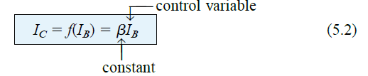
We know that for a bipolar junction transistor (BJT), the output collector current IC and the control input base current IB are related by the parameter beta, which is assumed to be constant for an analysis.
Referring to the equation below, we find a linear relationship existing between IC and IB. If we make the IB level 2x, then IC also doubles proportionately.
But sadly, this convenient linear relationship may not be achievable in JFETs across their input and output magnitudes. Rather, the relationship between the drain current ID and the gate voltage VGS is defined by Shockley’s equation:
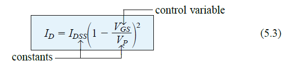
Here, the squared expression becomes responsible for the non-linear response across the ID and VGS, which gives rise to a curve growing exponentially, as the magnitude of VGS is decreased.
Although a mathematical approach would be easier to implement for the dc analysis, the graphical way might require a plotting of the above equation.
This can present the device in question and the plotting of the network equations relating to the identical variables.
We find the solution by looking at the point of intersection of the two curves.
Remember, that when you use the graphical method, the characteristics of the device remains unaffected by the network where the device is implemented.
As the intersection between the two curves changes, it also changes the network equation, but this has no effect on the transfer curve defined by the above Eq, 5.3.
Therefore, in general we can say that:
The transfer characteristic defined by Shockley's Equation is not affected by the network where the device is implemented.
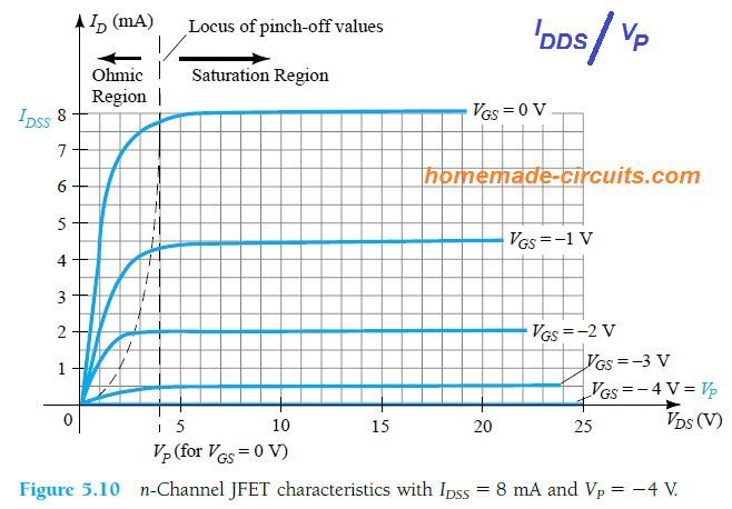
We can get the transfer curve using Shockley's equation, or from the output characteristics as depicted in Fig.5.10
In the figure below, we can see two graphs. The vertical line measures milliamperes for the two graphs.
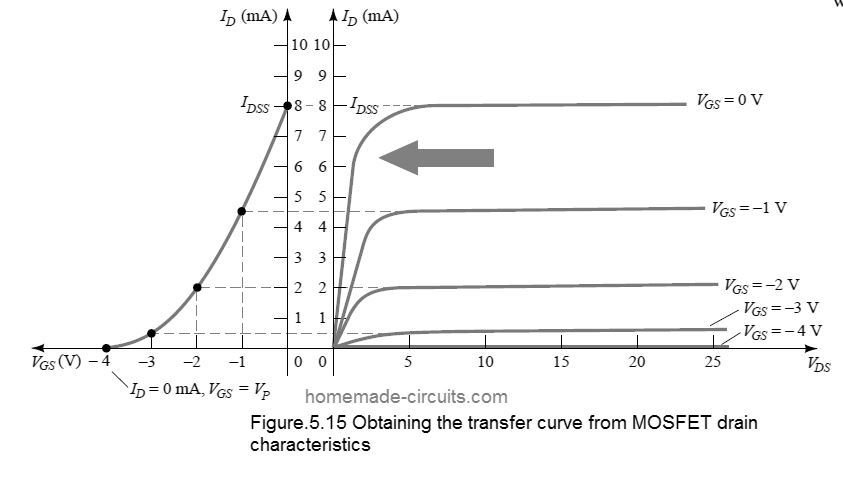
One graph plots the drain current ID versus drain-to-source voltage VDS, the second graph plots the drain current versus gate-to-source voltage or ID vs VGS.
With the aid of the drain characteristics shown at the right side of the "y" axis,we are able to draw a horizontal line starting at the saturation region of the curve shown as VGS = 0 V upto the axis shown as ID.
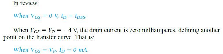
The current levels thus achieved for the two graphs is IDSS.
The point of intersection on the curve of ID vs VGS will be as given below, because the vertical axis is defined as VGS = 0 V
Note that the drain characteristics show the relationship between one drain output magnitude with another drain output magnitude, wherein the two axes are interpreted by variables in the same region of the MOSFET characteristics.
Thus, transfer characteristics can be defined as a plot of a MOSFET drain current versus a quantity or a signal acting as an input control.
This consequently results in a direct "transfer" across input/output variables, when the curve is used at the left of Fig 5.15. If it had been a linear relationship, the plot of ID vs VGS would have been a straight line across IDSS and VP.
However, this results in a parabolic curve due to the vertical spacing between the VGS stepping over the drain characteristics, that decreases to an appreciable extent as VGS gets increasingly negative, in Fig 5.15 .
If we compare the space between VGS = 0 V and VGS = -1V with that of between VS = -3 V and the pinch-off, we see that the difference to be identical, although it's a lot different for the ID value.
We are able to identify another point on the transfer curve by drawing a horizontal line from VGS = -1 V curve until the axis of ID and subsequently extending it to the other axis.
Observe that VGS = - 1V at the bottom axis of the transfer curve when ID = 4.5 mA.
Also note that, in the ID definition at VGS = 0 V and -1 V, the saturation levels of ID are used, while the ohmic region is neglected.
Moving further ahead, with VGS = -2 V and - 3V, we are able to finish the transfer curve plot.
How to Apply Shockley's Equation
You can also directly achieve the Fig 5.15 transfer curve by applying Shockley's Equation (Eq.5.3), provided the values of IDSS and Vp are given.
The IDSS and VP levels define the limits of the curve for the two axes, and necessitates only the plotting of a few intermediate points.
The genuineness of the Shockley’s equation Eq.5.3 as a source of the transfer curve of Fig 5.15 can be perfectly expressed by inspecting certain distinctive levels of a particular variable and then identifying the corresponding level of the other variable, in the following way:
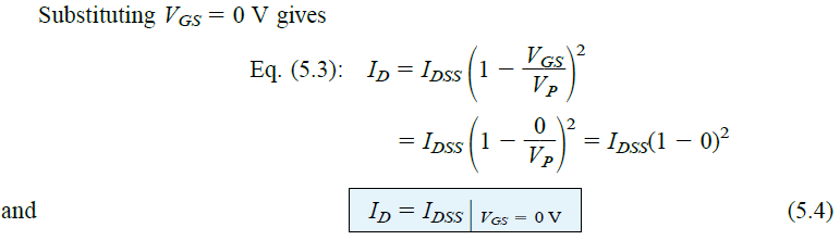
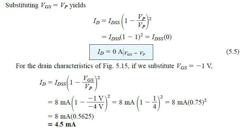
This matches the plot shown in Fig.5.15.
Observe how carefully the negative signs for VGS and VP are managed in the above calculations. Missing out even a single negative sign could lead to a totally erroneous result.
It is pretty clear from the above discussion, that if we have the values of IDSS and VP (which can be referred from the datasheet), we can quickly determine the value of ID for any magnitude of VGS.
On the other hand, through standard Algebra we can derive an equation (via Eq.5.3), for the resulting VGS level for a given level of ID.
This could be derived quite simply, to get:
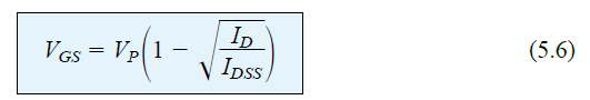
Now let us verify the above equation by determining the VGS level that produces a drain current of 4.5 mA for a MOSFET having the characteristics matching Fig 5.15.
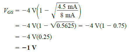
The result verifies the equation as it conforms with the Fig.5.15.
Using the Shorthand Method
Since we need to plot the transfer curve quite often, one might find it convenient to get a shorthand technique for plotting the curve. A desirable method would be that allows the user to plot the curve quickly and efficiently, without compromising on accuracy.
The equation 5.3 that I have explained above is designed such that particular VGS levels produces levels of ID that can be remembered for utilizing as plot points while drawing the transfer curve. If we specify VGS as 1/2 of the pinch-off value VP, the resultant ID level can be determined using Shockley's equation in the following manner:
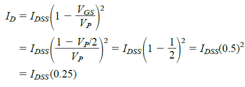
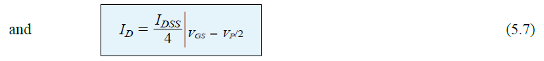
It must be noted that the above equation is not created for a specific level of VP. The equation is a general form for all VP levels for so long as VGS = VP/2. The result of the equation suggests that the drain current will be always 1/4th of the saturation level IDSS as long as the gate-to-source voltage has a value that's 50% less than the pinch-off value.
Please note that the level of ID for VGS = VP/2 = -4V/2 = -2V as per the Fig.5.15
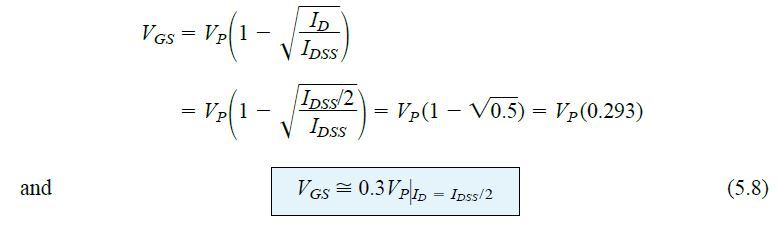
Opting ID = IDSS/2 and substituting it into Eq.5.6 we get the following results:
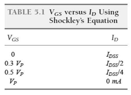
Although further number points can be established, sufficient level of accuracy can be simply achieved by drawing the transfer curve using only 4 plot points, as identified above and also in Table 5.1 below.
In most cases we can employ just the plot point using VGS = VP/2, while the axis intersections at IDSS and VP will give us a curve sufficiently reliable for most of the analysis.


Need Help? Please Leave a Comment! We value your input—Kindly keep it relevant to the above topic!