In this post I have explained MOSFET avalanche ratings, and learn how to understand this rating in the datasheet correctly, how the parameter is tested by the manufacturer, and measures to protect MOSFETs from this phenomenon.
The avalanche parameter not only helps to verify the devices ruggedness, it additionally helps filtering out weaker MOSFETs or the ones which are more susceptible or at risk of a breakdown.
What is MOSFET Avalanche Rating
MOSFET avalanche rating is the maximum tolerable energy (millijoule) a MOSFET can withstand, when its drain-source voltage exceeds the maximum breakdown voltage (BVDSS) limit.
This phenomenon normally occurs in MOSFET switching circuits with inductive load across the drain terminal.
During the ON periods of the switching cycles, the inductor charges, and during the OFF periods the inductor releases its stored energy in the form of back EMF across source-drain of the MOSFET.
This reverse voltage finds its way through the MOSFET's body diode, and if its value exceeds the device's maximum tolerable limit, causes intense heat to develop within the device causing harm or a permanent damage to the device.
When was MOSFET Avalanche Introduced
The parameter Avalanche Energy and UIS (unclamped inductive switching) current was in fact not included in MOSFET datasheets before the 1980s.
And that's when it evolved into not only a datasheet specification, but a parameter which many consumers began demanding that the FET be tested before passing the device for production, especially, if the MOSFET is being designed for power supply or switching implementations.
Therefore it was only after 1980s that the avalanche parameter began appearing in the datasheets, and then promotion technicians began understanding that the bigger the avalanche rating was, the more competitive the device appeared to be.
The engineers began determining techniques to experiment with the parameter by tweaking few of its variables, which were used for the testing process.
Generally speaking, the bigger the avalanche energy, the more durable and strong the MOSFET turns into. Therefore larger avalanche rating, represents stronger MOSFET characteristics.
Most FET datasheets will normally have the avalanche parameter included in their Absolute Maximum Ratings Table, which can be found directly on entry page of the data sheet. Especially, you can view the parameters here written as Avalanche Current and Avalanche Energy, Eas.
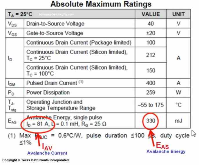
Therefore, in datasheets MOSFET Avalanche Energy is presented as the quantity of energy the MOSFET is able to tolerate while it is being subjected to the avalanche test, or when the MOSFET's maximum breakdown voltage rating is crossed.
Avalanche Current and UIS
This maximum breakdown voltage rating is determined through the Avalanche Current Test, which is accomplished through an Unclamped Inductive Switching test or the UIS test.
Hence when engineers discuss about UIS current, they may be referring to the Avalanche Current.
An Unclamped Inductive Switching test is performed to figure out the current and thereby the avalanche energy that could trigger the MOSFET failure.
As mentioned earlier, these magnitudes or ratings are hugely dependent on testing specifications, particularly, the inductor value applied at the time of the test.
Test Set Up
The following diagram shows a standard UIS test circuit set up.
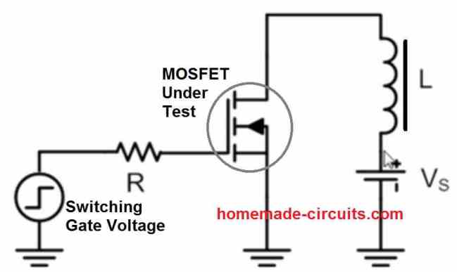
Thus we see a voltage supply in series with an inductor, L, which is also in series with the MOSFET under test. We can also see a gate driver for the FET whose output is in series with a FET gate resistor R.
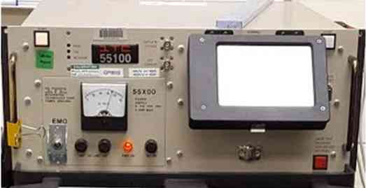
In the below image, we find, the LTC55140 controller device, which is used in Texas Instrument lab to evaluate the UIS characteristics of the FET.
The UIS characteristic subsequently helps not only to find out the FET datasheet rating, but also the value utilized to scan the FET in the final testing procedure.
The tool allows tweaking the load inductor value from 0.2 to 160 millihenries. It allows the adjustment of the the drain voltage of the MOSFET under test from 10 to 150 volts.
This, as a result makes it possible to screen even those FETs which are rated to handle only 100 volt breakdown voltage. And, it becomes possible applying drain currents from 0.1 to 200 amps. And this is the UIS current range which the FET may have to tolerate during the testing procedure.
Additionally the tool allows setting different ranges of the MOSFET case temperatures, from -55 to +150 degrees.
Testing Procedures
The standard UIS test is implemented through 4 stages, as illustrated in the following image:
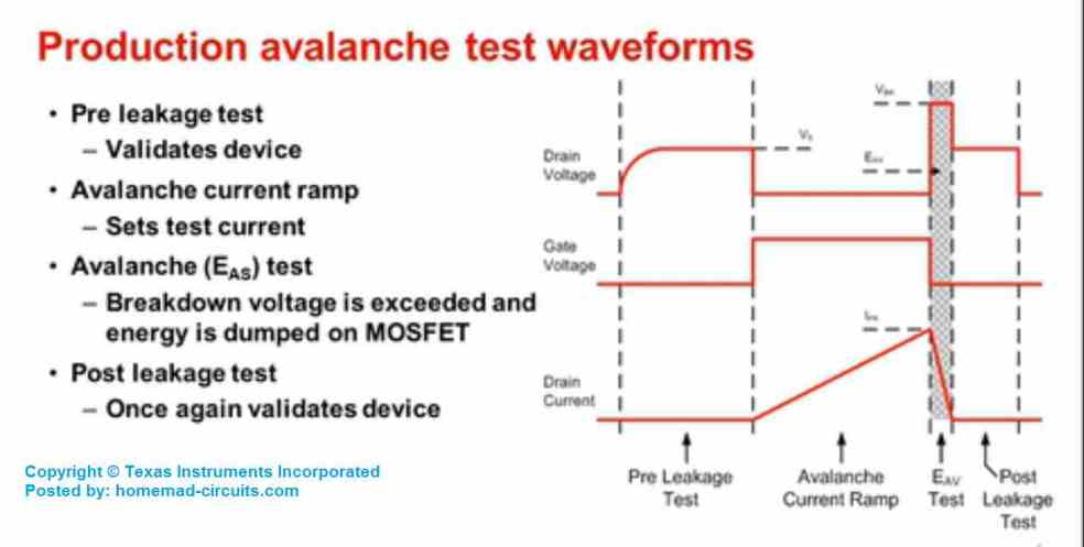
The first stage consists of the pre-leakage test, in which the supply voltage biases the FET drain. Fundamentally, the idea here is to try to ensure the FET is performing in the normal expected manner.
Thus, in the first stage the FET is held switched off. It keeps the supply voltage blocked across the daim-emitter terminals, without experiencing any kind of excessive leakage current flowing through it.
In the second stage, which is known as the Avalanche Current ramp up, the FET is switched ON, which causes its drain voltage to drop. This results in the current to increase gradually through the inductor with a constant di/dt. So basically in this stage, the inductor is allowed to charge up.
In the the third stage, the actual avalanche test is carried out, where the FET is practically subjected to the avalanche. In this stage the FET is turned off by removing its gate bias. This results in a massive di/dt getting through the inductor, causing the FET drain voltage to shoot high above the breakdown voltage limit of the FET.
This forces the FET to go through the avalanche surge. In this process, the FET absorbs the whole energy generated by the inductor, and stays shut off, until the 4rth stage is executed, involving the post leakage test
In this 4rth stage the FET is once again subjected to the a repeat avalanche test, just to be sure whether the MOSFET is still behaving normally or not. If it does, then the FET is deemed to have passed the avalanche test.
Next, the FET has to go through the above test many more times, wherein the UIS voltage level is gradually increased with each test, until the level where the MOSFET is unable to withstand and fails the post-leakage test. And this current level is noted to be the MOSFET's maximum UIS current withstanding capability.
Calculating MOSFET Avalanche Energy
Once the maximum UIS current handling capacity of the MOSFET is realized, at which the device breaks down, it becomes much easier for the engineers to estimate the quantity of energy that is dissipated through the FET during the avalanche process.
Assuming, the entire energy stored in the inductor was dissipated into the MOSFET during the avalanche, this energy magnitude can be determined using the following formula:
EAS = 1/2L x IAV2
EAS gives us the magnitude of energy stored inside the inductor, which is equal to 50% of the inductance value multiplied by the current squared, flowing through the inductor.
Further on, it was observed that as the inductor value was increased, the amount of current that was responsible for the MOSFET breakdown actually decreased.
However this increase in inductor size in fact offsets this reduction in current in the above energy formula in a way that the energy value literally increases.
Avalanche Energy or Avalanche Current?
These are the two parameters, which can be confuse the consumers, while checking a MOSFET datasheet for avalanche rating.
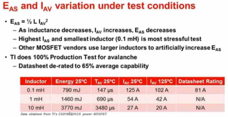
Many of the MOSFET manufacturers intentionally test the MOSFET with larger inductors, so that they are able to boast a larger avalanche energy magnitude, creating an impression that the MOSFET is tested for withstanding huge avalanche energies, and therefore has an increased durability to avalanche.
But the above method of using larger inductor looks misleading, that is exactly why the Texas Instruments engineers test with smaller inductance in the order of 0.1 mH, so that the MOSFET under test are subjected to higher Avalanche current and extreme breakdown stress levels.
So, in datasheets, it is not the Avalanche energy, rather Avalanche current that should be bigger in quantity, which displays better MOSFET ruggedness.
This makes the final testing highly stringent and enables filtering out as many weaker MOSFETs as possible.
This test value is not only used as the final value before the FET layout is passed for the production, but this is also the value which is entered in the datasheet.
In the next step, the above test value is derated by 65%, so that the end user is able to get a wider margin of tolerance for their MOSFETs.
So for example, if the tested avalanche current was 125 Amps, the final value which is entered in the datasheet happens to be 81 Amps, after the derating.
MOSFET Avalanche Current vs Time Spent in Avalanche
Another parameter that is associated with power MOSFET and mentioned in datasheets, especially for the MOSFETs designed for switching applications is the Avalanche Current Capability versus Time Spent in Avalanche. This parameter is normally shown with respect to the MOSFET's case temperature at 25 degrees. During the testing the case temperature is increased to 125 degrees.
In this situation the MOSFET's case temperature of the MOSFET gets very close to the actual junction temperature of the MOSFET's silicon die.
In this procedure as the device's junction temperature is increased, you may expect to see a certain amount of degradation which is quite normal? However, if the result shows a high level of degradation , that may indicate the signs of an inherently weak MOSFET device.
Therefore from a design viewpoint, an attempt is made to ensure that the degradation does not exceed over 30% for an increase in case temperature from 25 to 125 degrees.
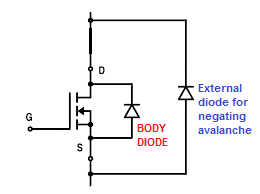
How to Protect MOSFET from Avalanche Current
As I have explained from the above discussions, avalanche in MOSFETs is developed due to high voltage inductive back EMF switching through MOSFET's body diode.
If this back EMF voltage exceeds the maximum rating of the body diode, causes extreme heat generation in the device and subsequent damage.
This implies that if the inductive EMF voltage is allowed to pass through an external suitably rated bypass diode, across the drain-emitter of the FET may help avert the avalanche phenomenon.
The following diagram suggests the standard design of adding an external drain-emitter diode for reinforcing the internal body diode of the MOSFET.
Courtesy: MOSFET Avalanche


Comments
I need to replace the Mosfert of a motor ignition coil, but the MOSFET burns from the repetitive spikes of -600V
I don’t have instrumentation to measure inductance across the coil, but I know the impedance is 1 ohms at 12 volts.
What should I keep in mind when analyzing a data sheet and choosing a suitable replacement for inductive loads?
From already thank you very much.
You can probably refer to the following post and add a few external safety measures to your mosfets, as per the recommendations:
How to Protect MOSFETs – Basics Explained
In datasheet, you must check 3 basic aspects to match an existing mosfet.
VDS or the maximum darin to source voltage
ID or the maximum drain current
RDSon or the minimum resistance across drain source of the device.
In a step down power transformer,
If we short 9VAC and 12VAC wires in the point ‘a’ as shown above,
Can we connect and use the above topology?
What is the impact on the secondary and primary windings?
Please check in below Link….
https://drive.google.com/file/d/1pWcgwqwr0jmjhOhzMSGTY1nLf__tM60H/view?usp=sharing
shorting any of the winding of the transformer will cause heating up of the transformer.
Dear sir,
Please sir, how can I know the external diode value suitable for the avalanche protection?
It will depend on the maximum working current of the system, or the load
Okay sir, thank you very much.
Please sir, in order to know the value of the diode to be used for the protection:
Please sir, what is the max working current for this system below?
* I want to use the Elite600VA UPS transformer.
* From your replies on my last questions on pure sine wave inverter circuit using Ic 4047, I want to use four 10W/220V LED light bulbs and one 8W/220V LED light bulb on the 12V, 25Ah lead acid battery for 3 or 4 hours.
2. Please sir, what is the diode value I can use for the system?
3. Please sir, show how to calculate to know the working current of the system for the choice of diode.
Godfrey, The diode can be 4 amp diode, or 1N5402/1N5408 will do.
I have explained you in details in the previous comments regarding the working current calculations, which is 4 amps in your case.
Thank you very much sir.