In this post I have explained a few very simple boost converter circuits using only BJTs, or transistors. Let's learn more.
What is a Boost Converter
A DC boost converter circuit is designed for stepping-up or boosting a small input voltage levels to a desired higher output voltage level, hence the name "boost" converter.
Since these circuits basically step up a low voltage to a higher voltage levels, they are also know as step-up converters.
Although a boost converter circuit may involve many complex stages and calculations, here we will see how the same could be built using minimum number of components, and with effective results.
Basically a boost converter works by oscillating current though a coil or inductor, wherein the voltage induced in the inductor is transformed into a boosted voltage whose magnitude is dependent on the number of turns and PWM of the oscillation frequency.
Basic Working Principle of Boost Converter
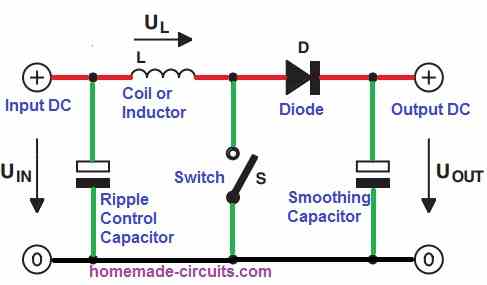
Referring to the figure above, the basic working principle of a boost converter topology can be understood from the following points:
When the switch S is switched ON, the coil voltage UL becomes equal to the input voltage and the current through the coil begins increasing linearly.
Next, if the switch S is turned OFF, the coil ensures that current through it keeps flowing independent of how much the output voltage rises. The current at this moment flows via diode D.
In this situation, the coil voltage UL is negative and the output voltage is higher than the input voltage.
As a result, the current flowing through the coil decreases linearly. During this period, the coil supplies the output with a stepped-up, boosted voltage.
After this, if the switch S is switched ON again, the process repeats. The above process repeats continuously as long as the switch S is switched ON/OFF repeatedly.
This causes the output to get a continuous supply of a stepped-up voltage. The smoothing capacitor makes sure the boosted voltage is filtered correctly and is a pure DC.
You may also like: Make this 1.5 V to 3.6 V boost converter for LED flashlights
A boost converter (also called step-up converter) is a DC to DC converter circuit which is designed to convert an input DC voltage into an output DC voltage with a level that may be much higher than the input voltage level.
However the process always conserves the relation P = I x V, which means that as the output of the converter steps up the input voltage, the output proportionately undergoes a reduction in current, which causes the output power to be almost always equal to the input power or less than the input power.
Simple 5 V to 12V Boost Converter Circuit using 2N2222
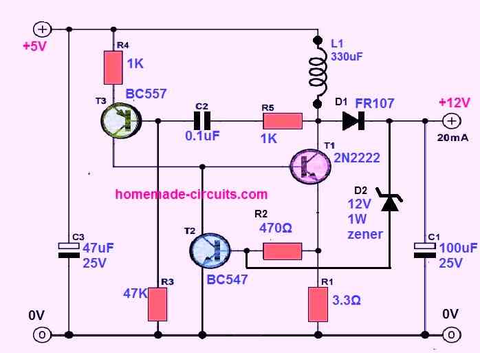
In the first concept as shown in the figure above, the input DC supply can be anywhere between 3 V and 5 V.
We can adjust the output voltage to 12 V or some other desired voltage by tweaking the zener diode D2.
So, when output voltage tends to increase excessively, T2's operating point shifts, causing T1 to switch on for a shorter duration of time (or maybe not at all).
We can expect the stepped-up output voltage to be around 12.6V at a 20 mA output current. The input current at a 5 V input voltage will be around 64 mA.
This translates to an efficiency of 77%, which is not bad at all for such a straightforward circuit.
How to get +5V, -5V Dual Supply from 1.2 V
If you are looking for a circuit to boost 1.2 V NiCd supply to 5 V then you can use this second circuit below.
Moreover, this circuit will allow you to get a dual +5V and -5V supply from a 1.2 V DC single supply input.
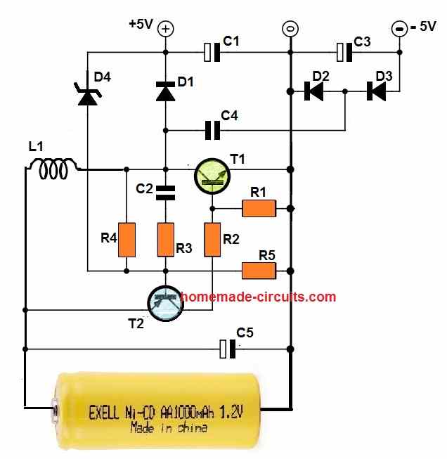
Parts List
- All resistors are 1/4 watt 5% unless specified
- R1, R5 = 1 K
- R2, R3 = 100 Ohms
- R4 = 2.2 K
- Capacitors
- C1 = 10 uF / 25 V Electrolytic
- C2 = 0.01 uF Ceramic Disc
- C3 = 1 uF / 25 V Electrolytic
- C4 = 0.1 uF Ceramic Disc
- C5 = 10 uF / 25 V Electrolytic
- Semiconductors
- D1, D2, D3 = FR107
- D4 = 5.1 V 1/2 watt zener diode
- T1 = 2N2222
- T2 = 2N2907
- Inductor
- L1 = 270 uH 500 ma
The step up converter is basically formed using T1, L1 and D1.
Zener diode D4 functions as a feedback at the base of transistor T2 and provides the required stabilization for the circuit.
The maximum current output capacity of this circuit is around 10 mA at +/- 5V.
The circuit will provide a maximum efficiency of 60% which does not looks too impressive. However with an input DC of just 1.2 V you cannot except more than this.
1.5 V to 30 V Boost Converter using a single BJT
The third boost converter circuit shown below uses a joule thief flyback topology.
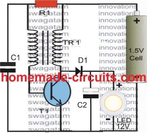
Parts List
- R1 = 1K 1/4 watt
- D1 = 1N4148 or a Schottky diode such as FR107 or BA159
- T1 = any NPN power BJT such as TIP31, 2N2222, 8050 or BC139 (on heatsink)
- C1 = 0.0047uF
- C2 = 1000uF/25V
Inductor is built using 20 turns each of super enameled copper wire on a ferrite torroid T13. Wire thickness can be as per the output current requirement.
In the above design a single BJT and an inductor is all that's needed for visualizing an incredible 1.5V to upto 30V boost.
The circuit works using a joule thief concept and utilizes an inductor in the flyback mode for generating the specified high efficiency output .
Using a flyback concepts allows the two side of the transformer isolated and ensures better efficiency, since the load is able to operate during the OFF time of the BJT, which in turn prevents the BJT from overloading.
While experimenting I found that adding C1 drastically improved the performance of the circuit, without this capacitor the output current did not look too impressive.


Need Help? Please Leave a Comment! We value your input—Kindly keep it relevant to the above topic!