In this post we talk about a parametric equalizer circuit which can be used to enhance a music output to outstanding levels, much better than any standard graphic equalizer output.
Advantages
The main advantage of a parametric equalizer is that it allows you to modify the frequency and the "Q factor" across a wide range while also controlling the gain, which is not possible in most graphic equalizer circuits.
Furthermore, in most cases, a couple of parametric equalizers per channel may outperform a complex graphic equalizer. Therefore, the circuit design discussed in this article can produce extremely beneficial results by enhancing the music input quality to outstanding levels.
Specifications
The mentioned parametric equalizer is a high-performance gadget that may be used with even the most unconventional hifi system. The boost and cut range specifications on the device were zero to slightly over 20dB, with a Q factor variable from 1 to 25, and a frequency range of 50Hz to 11kHz.
The Gain and Q tests were taken at 1kHz, however the response uniformity was found to be superb over the whole frequency range.
Since frequencies lower than 50Hz is mostly never preferred, the lower range specification of this circuit is excellent for the majority of the audio applications. The upper range spec of 11 kHz is also great as it decreases the chance of harming tweeters if the equalizer is set to a powerful boost at high frequencies (unless a correction is being done for a trough in the response). However, as detailed later in the article, the frequency range could well be easily changed, as desired, for this circuit.
A high-gain, high-Q parametric equalizer is very effective for 'enhancing' recordings. The most typical changes can be raising frequencies that are not available in the original music and eliminating undesired frequencies, such as noise.
Parametric equalizers like this are also great for techno music. For starters, this parametric equalizer may be used as a so-called passive filter for illustrative music synthesis, boosting a music spectrum, or spectrum of frequencies that are typical of the instrument being mimicked.
Because the frequency changes they may create are fairly striking, particularly at higher gain levels, these equalizers are now frequently utilized as an effects unit.
Circuit Description
The following diagram depicts the full circuit schematic for one channel of the parametric equalizer. The equalizer's main feature is a band pass filter, which is built around ICs 3a, 3b, and 3c, which are configured in a 'state-variable' topology.
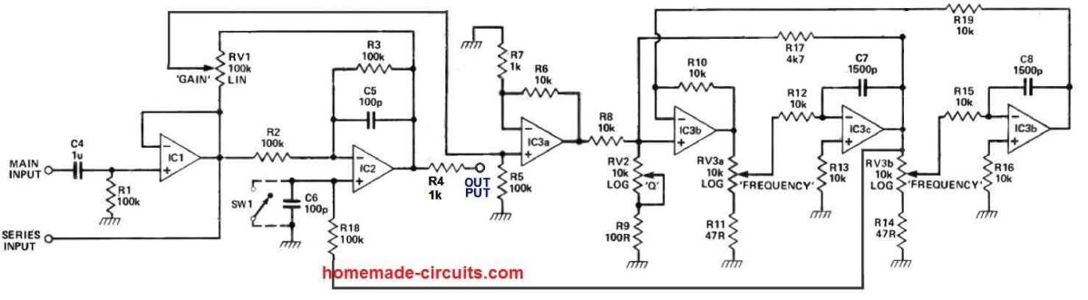
The band pass is obtained from the output of IC3c, and the filter's center frequency is controlled by the capacitors C7 and C8 which work like integrators, along with the resistance defined by the ganged potentiometer RV3.
The frequency range using 1500pF capacitors is 50Hz to 11kHz, and this range may be changed by adjusting each C7 and C8 values. For example, If 1000pF capacitors were used instead, the frequency range would be between 75Hz to 16.5kHz, whereas 2000pF capacitors would cause the frequency range to be 35Hz to 7.5kHz.
Returning to the input stage, the music input is AC linked to IC1, which is basically a buffer stage that provides a low impedance to the gain control, RV1. Resistor R1 determines the circuit's input impedance.
The processed signal subsequently goes to the output through the unity gain amplifier IC2.
The filter section becomes disabled when switch SW1 is flipped to short the non-inverting input of IC2 to ground.
The filter receives its input through RV1, which has its one end wired to the original non-inverted signal at the IC1 output, and the other end hooked up to the inverted signal at the IC2 output.
The wiper of RV1 provides signal input to the band pass filter, while RV3 decides what frequency elements are processed by the filter and supplied back into IC2's non-inverting input.
As a result, when RV1's wiper is nearer to IC1's output (the original input music signal), higher amounts of the original signal's specified frequency band is added (boosted) to the original signal at IC2.
On the other hand when the RV1 wiper is nearer towards the IC2 output, the result is to subtract (cut) the original signal in IC2.
Although, the effect is similar to that of a traditional graphic equalizer, the flexibility to modify frequency throughout the whole range is a great benefit of this parametric equalizer.
A variable Q is another element that must be included in a parametric equalizer; the greater the Q, the more peaked the filter response will be.
Having a lot of feedback increases Q, and getting a high Q without allowing the filter to oscillate is one of the key advantages of implementing a state-variable-filter.
The ratio of R8 and R17 control the circuit's Q, if RV2/R are not included. However, changing these resistors would also change the circuit's gain unless the configuration is changed and dual potentiometers are introduced to vary both resistor values. This issue is solved by boosting the gain before R8, then changing Q by blunting the feedback signal through RV2.
How to Use
The parametric equalizer circuit has unity gain when the wiper of the gain control pot is in the middle position or the by-pass point is wired with the ground, which means the signal out value is the same as the signal in value. As a result, the input signal needs be pre-amplified, and with many audio amplifiers, the monitor output is the best place to start.
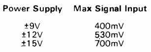
The maximum signal level that may be utilized is determined to some extent by the power supply and to some extent by the application.
The cut and boost controls are solely configured to correct for frequency response shortcomings in hi-fi and many recording scenarios, ensuring an essentially flat response.
Without depending on the power supply used, the parametric equalizer circuit will deal with the signal levels typically found in these types of Hi-Fi systems.
In case this parametric equalizer is being utilized for special effects and the gain is adjusted to either extremes, the highest levels of input music signal illustrated in the below given table are recommended to prevent clipping.
If you don't have an audio analyzer device with you, you may have to start by tweaking the knobs and judging the response by ear, much like you do with your tone controls.
Begin with the Q control at or around the lowest setting, then gently increase or decrease gain from the center position, and then slowly move the frequency control clockwise.
The results will astound you, and you will quickly find the ideal settings for your setup. Because the spectrum of frequencies being boosted or cut is considerably smaller as Q is raised, the influence of the gain control is often less perceptible to the ear unless it is focused on certain consistent frequency of the music.
By-Pass Switch
A SPST switch can be connected between the 'by-pass switch, SW1' and '0V' terminals as indicated in the circuit diagram (parallel to C6). Whenever the switch is turned ON, the non-inverting input of IC2 is grounded, and the original input signal flows through the equalizer without being influenced by the potentiometer adjustments.
The switch can be very useful for checking the effects of the circuit, simply by switching the SW1 ON/OFF. The switch will quickly enable you to analyze the difference in the output results of this parametric equalizer circuit, simply by toggling the switch in and out.
About the Series Input Terminal
In a high-fidelity (hifi) system, using three parametric equalizers is generally more effective than a graphic equalizer with ten or more channels.
When connecting multiple units per channel, they must be connected in a series. The initial unit receives the signal from the "Main Input" and passes its output to the "Series Input" of the second unit.
This process continues until the last unit, whose output connects to the output socket of the channel. The second and following units do not require IC1, C4, and R1 components. If these components are already installed, the unit will not function unless IC1 is removed from the additional equalizers.

Comments (29)
hello
one type of parametric Equalizer/
equalizer needed-
flat output with Bass boost.
bass boost – around 60Hz with
Q= approx 8-10.
if you have idea please provide or give link.
Thanks
Hi, sorry, I do not have this specific design, but i think you can customize the part values the above explained parametric equalizer to suit your desired specifications…
Hello Swagatam,
I had a question about the calculations to find the cut-off frequencies of the bandpass filter. What calculations did you make to find the capacitor values according to the desired frequency? I want to be able to change the frequency between 100Hz and 2kHz, but after several attempts I can’t find the solution.
In order to modify the Gain and the Q, which parameters do I need to adjust? What calculations do I need to perform, if any? Because I also need to vary these two parameters independently.
Thanks for your help
Thank you Pigi,
However,, unfortunately, calculations for this circuit is not available to me. This circuit was not designed by me, rather was contributed by an external source.
OK thank you, but do you know how to have this equalizer with a frequency changing between 100Hz and 2kHz ?
The above equalizer will easily handle frequencies between 100 Hz and 2 kHz, and produce the intended outcome as set by the relevant pots.
All right, but I can’t find the values to obtain a center frequency varying between 100Hz and 2kHz.
Can you please help me find the solution as I’m a bit lost?
Sorry Pigi, unfortunately I do not have the required information with me right now for this circuit, I think you may have to find it through some practical experimentation.
hello Swagatam, I desperately want to build this circuit but i am a total noob when it comes to electronics. From what i undestand, the ‘main input’ receives the audio signal, and the ‘series input’ is for combining multiple channels. So, where is the V-in? How do i feed the voltage into this circuit?
Hello Onur,
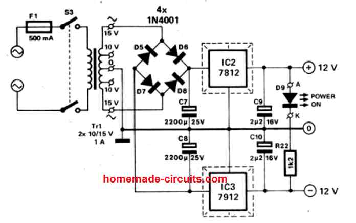
You will need a dual power supply circuit to operate the above parametric circuit. You can try the following dual power supply design:
The positive (+) supply will go to all the (+) or Vcc terminals of the op amps.
The negative (-) supply will to to all the (-) or Vss terminals of the opamps.
The ground supply will go to all the points that are marked as ground in the above parametric circuit diagram
Let me know if you have any further doubts?
thank you very much, now it makes sense. Let’s see if i’ll be able to get my hands on a dual power supply 🙂
Sure, no problem, all the best to you!!
alright, i have a couple more questions. Is there any problem with using a single TL072 for IC1 and IC2, and a TL074 for IC3a-b-c-d, since these have multiple opamps inside, or should I use 6 seperate chips for each individual IC’s? By the way I can’t see C1,C2 and C3 on the circuit. Do I just skip that?
You can definitely use quad opamp ICs to fulfill the opamp count, no need of using individual opamps.
Yes, you can ignore those caps, they were most probably included in a different preamplifier module.
Thank you ! Swagatam, could you tell me the formula for frequcency response? Im gonna make it for bass guitar so the range wich interest me gonna be between 60 to 3k Hz .
Hi Andrzej, sorry, i do not have the formula for calculating frequency response. I think the frequency response adjustments can be better done with some practical experimentation, or with some trial and error.
How is the series input used?
I have updated the information at the end of the post.
Why would extra buffers be an issue in this system?
Hi! I’m a music/electronics hobbyist interested in building this parametric eq circuit.
Can you share PCB layout please.
Hi, sorry, I do not have the PCB design for this project.
I assume the second IC3b (at far right) is supposed to be IC3d …
You are absolutely right, I hope the other readers will take a note of this!
2 questions about this design:
1. What ICs are used, and does the design require different opamps at the various stages?
2. My understanding is that this circuit carries unbalanced audio – what, if any, modification to the design would be required to carry balanced audio?
Thanks!
The op amps can be from 6nos of TL072 or LM358.
Sorry i am not sure about your second question since I am not an audio expert.
I need an audio equilizer circuit that will boost the higher frequencies of the human hearing spectrum.
Getting older, I am loosing some high frequency hearing. Not using hearing aids yet. But, as a private pilot the attenuation of the higher frequencies makes understanding some air traffic controllers more difficult. So I need a circuit to boost the higher frequencies: maybe 1 to 4 khz range? The headphones we use in airplanes have an impedance of 150 ohms. I would like to plug my aviation headsets into the audio equilizer and plug the equilizer into aircraft audio panel. I have a USB plug for power or batteries could be used. Would you have a circuit that would do this?
I think a treble booster circuit would perfectly satisfy your requirement.
You can try the “treble booster circuit” as explained in the following article:
https://www.homemade-circuits.com/simple-tone-control-circuits/
where does REM to be connected?
REM stands for “remote” but this has no connection with the above explained circuit.