The IC 4040 is technically a 12-stage binary ripple counter chip, in simple words a device which will produce a calculated delayed frequency output in response to every pulse applied at its clock input. This delay is incremented at the rate of 2n where n is the pinout order in the sequence of its outputs.
Main Technical Specifications
The main features and specifications of the IC may be understood as follows:
Fully buffered 12 outputs which divide the input clocks at the rate 2n where n = the pinout order starting from Q0 until Q11.
The above sequencing of the outputs happens in response to every falling edge of the clock applied at its clock input CP pinout. The IC will respond even to a relatively slow falling clock pulse as effectively.
A single asynchronous master reset (MR) input which resets all outputs to zero when a high logic is applied, whereas a constant low logic enables the IC to stay active.
The IC becomes fully operational with Vdd as low as of 3V and sustains a constant operational characteristic even at voltages around 15V.
Let's examine the parameters which shouldn't be exceeded for the IC 4040
- Supply Voltage (Vdd) = Typically between 3 V and 15 V, 18 V being the maximum limit.
- Input Voltage (Vi) = The voltage that may be applied at the inputs such as CP, MR etc should be typically below Vdd or at the most = Vdd + 0.5V
- Optimal Operating Current Requirement = 50mA since so many outputs are involved and each output
Pinout Details
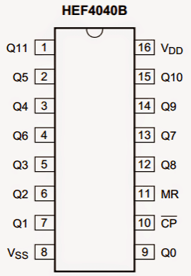
The diagram above depicts the pinout configuration of the IC 4040, they may be evaluated as given under:
Pinouts Q0 to Q11 are the outputs of the IC.
- Vss is the ground pin.
- Vdd is the positive pin.
- MR is the reset pinout
- CP is the clock input.
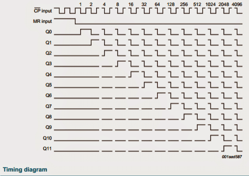
Timing Sequence
Now let's analyze the output timing sequence of the IC 4040. As shown in the following diagram, we are able to see and understand the following details:
As long as the MR input is high, the IC outputs produce no response. As soon as it goes low, the IC starts responding and counting the input clock at the CP input.
The first output pin Q0 goes high after 2n clock at CP, that's = 20 = 1, meaning Q0 becomes high at the falling edge of the first pulse and goes low in response to the falling edge of the subsequent clock and so on.
Similarly Q1 goes high after 21 = 2, meaning it goes high as soon as a falling edge of the second clock is detected and goes low at the falling edge of the 4th subsequent clock and so on.
Identically Q2 goes high and low after 22 = 4th clock's falling edges, and so on.
The above sequence is continued until Q11, in response to the sustained clock inputs at CP .
It means if suppose the CP is clocked with a 1Hz pulse, Q11 would go high after 211 seconds or after 2048 seconds that's equal to 34 minutes approximately, just imagine the range of delay that you can achieve by simply increasing the clock input by seconds or perhaps by minutes.
Understanding Pinout Working with an Example
From the above explanation it is clear that the output pins divide the input clock input frequency with some magnitude determined by the Q number and by 2n .Let's try to understand this with an example, as I have explained below:
We will take the example of Q11 which is pin#1 of the IC 4040.
Q11 will divide the clock frequency by 211 = 2048.
This implies that the clock frequency applied on pin#10 will be divided by 2048 by the output pin#1 (Q11).
Suppose, we have a clock frequency of 2 Hz at pin#10, this will be divided 2048 at Q11.
Therefore, 2 / 2048 = 0.00097 Hz, which is equal to 1031 seconds.
Now, 2 Hz = 0.5 seconds.
Meaning, the 0.5 second ON/OFF delay at pin#10 of the IC will be converted to a 1031 seconds ON/OFF delay at Q11 of the IC.
The above calculation can be used to figure out the delays across all the other pinouts of the IC 4040.
Application Hints
From the above detailed analysis of the IC 4040 datasheet we can conclude that the IC is typically suited for all application which involve frequency division requirements or delayed time period generation requirements.
Therefore it could become specifically suited for frequency divider circuit applications, long duration timers, flashers and other such similar applications.
Summary
The main technical datasheet of the IC 4040 can be summarized as I have explained below:
Electrical Characteristics
The following are the electrical characteristics of the IC 4040:
- Supply Voltage (VDD): 3V to 18V
- Input Voltage (VIH): 2V to VDD
- Input Current (IIH/IIL): ±1µA
- Output Voltage (VOH/VOL): 0.5V to VDD-0.5V
- Output Current (IOH/IOL): ±10mA
- Power Dissipation (PD): 500mW
- Operating Temperature Range (TOPR): -55°C to 125°C
Timing Characteristics
The following are the timing characteristics of the IC 4040:
- Clock Pulse Width (tw): 20ns min
- Clock Rise/Fall Time (tr/tf): 10ns max
- Reset Pulse Width (twr): 10ns min
Applications
The IC 4040 is commonly used in the following applications:
- Digital frequency counters
- Timers
- Programmable dividers
- Frequency synthesizers
- Time delay circuits
- Clock generators

Questions & Answers
Hi.
I have the 4040 IC chip and want to make a simple clock divider to use with my synths.
Do you have a circuit diagram per chance please?
Hi,
I do not have a design in this blog, however, You can just feed the clock pulses to pin10 of the IC and get the divided outputs across the 12 output pins.
Thanks for responding,
Having had difficulties triggering the pin 10 clock pin of the 4040 binary counter. I searched
everywhere on the internet no mention found on RC negative end triggering pulse designs.
I finally succeeded in assembling an RC network ; Thanks to Ben Eater’s RC-push button network design described in his youtube EEPROM manual programming. Employing his RC design the push button neatly generated a negative edge pulse to trigger the clock pin (10) of the 4040 binary counter. This pulse as well triggered neatly write enable of the EEPROM.
I made sure to connect a debouncing 10nf capacitor across the push button pins.
Hello
I am having difficulty clocking the 4040 counter using a push button switch can you suggest any
clocking method?
Nick
What kind of problem are you facing? Keep CP grounded with a 10k resistor, and then apply the clocks.