The CD4027 is a dual J-K flip-flop IC with reset that can be used in a variety of digital logic applications. It has two independent flip-flops, each with a J and K input, a clock input, a reset input, and complementary Q and Q-bar outputs. The CD4027 operates on a wide range of supply voltages and is available in various package types.
The CD4027's maximum propagation delay, or the time it requires for an input change to be reproduced in the output, is 30 ns. The CD4027 is appropriate for battery-powered applications because to its low power consumption of 10 uA normal and 40 uA maximum.
The CD4027 can be procured in a variety of package configurations which includes PDIP, SOIC, and TSSOP. The datasheet provides a detailed description regarding the pin arrangement of the IC and the functions of each pinout.
Here is a brief datasheet of the IC CD4027:
Pinout Configuration
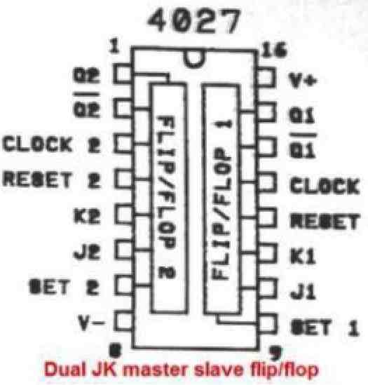
The pinout functioning of the IC 4027 can be understood from the following points:
As can be seen in the above IC 4027 pinout diagram, there are two sets of flip flop modules inside the IC. The pin#16 is the positive supply pin of the IC, and pin#8 is the ground supply pin of the IC.
Let's consider the left side flip flop pinouts and learn how these are assigned to work.
Pin#1, and pin#2 are the complementing outputs of the left side flip flop, named Q and Qbar. Whenever pin#1 is high, pin#2 is low and vice versa.
Pin#3 is the clock input of the left side flip flop. The above outputs alternately toggle ON/OFF in response to these clock signals.
Pin#4 is the reset pin of the left side flip flop. A ground potential on this pin will revert the output to their original condition. This pin is normally connected to the positive line via a resistor, and a push button is connected between this pin#4 and ground for implementing the resetting function.
Pin#5 is the K pinout of the left side flip flop.
Pin#6 is the J pinout of the left side flip flop.
When both the above J and K pinouts are held at low logic, the pin#1 and pin#2 are logic zero and logic 1 respectively.
When the J pin of the IC is toggled high, the output Q and Qbar can be turned opposite, in response to each clock pulse on pin#3 of the IC.
Meaning, suppose initially the Q output is logic zero and Qbar output is logic 1, this position will remain latched as long as the J and K pinouts are held low. When the J pin is made high, and pin#3 receives a single clock pulse, this will turn the Q output to high and Qbar output to logic low.
Now, in this position if the J pin is again reverted to low then the Q and Qbar output condition will get latched new position, and will not respond to the clock signal at pin#3.
If you want to revert the Q and Qbar position to it previous position, now you will have to switch the K pin of the IC to logic high.
Once the K pin is held to logic high, now the output will again respond to the clock pulse.
With a single clock pulse at pin#3 and K pin held high, the Q and the Qbar output will revert to its previous position.
Pin#7 is the SET pinout of the IC which is normally connected to the positive supply line in order to allow the normal functioning of the IC.
So this is how the the IC 4027 JK flip flop works.
The other side that the right hand side flip flop also has an identical set of pinouts which will produce exactly the same functioning as explained for the left side flip flop module.
Electrical Characteristics:
- Supply voltage range: 3V to 15V
- Maximum clock frequency: 16 MHz
- Maximum propagation delay: 30 ns
- Operating temperature range: -55°C to 125°C
- Power consumption: 10 uA typical, 40 uA maximum
- Output drive capability: 10 mA
Applications
Counters: A variety of synchronous binary counter designs for various purposes may be created using the IC 4027. Depending on the input, it can be used to count up or down.
Frequency Dividers: IC 4027 can be used as a frequency divider to create pulses with an output frequency that is lower than the input frequency.
Digital Circuits: IC 4027 is a multiplexer and demultiplexer that may be utilized in various applications. It is feasible to create intricate digital circuits that carry out a variety of tasks by interconnecting numerous ICs.
Frequency Modulation: A circuit that uses frequency modulation, or the act of changing a signal's frequency to transfer information, may be created using the IC 4027.
Pulse Width Modulation: IC 4027 could be used to produce a pulse width modulated (PWM) signals. This PWM can be implemented in numerous applications, for example like motor speed control, LED brightness control, and more.
Sequential Logic Circuits: IC 4027 is frequently used in applications like sequential logic circuits, which might include shift registers, counters, and frequency dividers.
Oscillators: IC 4027 could be also used to create oscillator circuits for generating periodic signals of a particular frequency.


Need Help? Please Leave a Comment! We value your input—Kindly keep it relevant to the above topic!