The CD4025 is a CMOS IC that contains three independent NOR gates, each with three inputs and one output. The device is designed for use as a digital buffer or inverter in high-noise environments due to its high noise immunity.
Electrical Characteristics:
- Wide supply voltage range: 3V to 15V
- High noise immunity: 0.45 VDD (typical)
- Low power consumption: 10 μA (maximum)
- High speed: 10 MHz (typical)
- Output drive capability: 10 LS-TTL loads
- Pin and functionally compatible with CD4001 and CD4075
Pinout Configuration
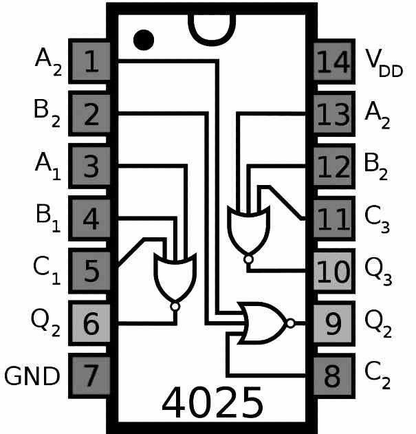
The pinout configuration of the IC 4025 are as I have explained below:
As shown in the above diagram, the IC 4025 is built with 3 special NOR gates, each having 3 inputs and one output.
When the 3 inputs are applied with high or low signals with a specific pattern, the output pin produces a low or high depending on the input pattern.
The pinout details of the IC 4025 are provide in the following table:
| VDD | 14 | Power | This pinout is the Supply Voltage input pin of the IC (+3 to +15V) |
| GND | 7 | Power | This is the Ground (0V) pinout of the IC |
| A1 to A3 | 1, 3, 13 | Input | These pinouts constitute Inputs A of the three NOR gates |
| B1 to B3 | 2, 4, 12 | Input | These pinouts serve as the Inputs B of the three NOR gates |
| C1 to C3 | 5, 8, 11 | Input | These pinouts work like the Inputs C of the three NOR gates |
| Q1 to Q3 | 6, 9, 10 | Output | These pinouts operate like the Outputs from the three NOR gates |
Truth Table
The following truth table explains how the outputs of each gate of the IC 4025 will operate when their inputs are fed specific positive or negative
| Input A | Input B | Input C | Output Q |
|---|---|---|---|
| 0 | 0 | 0 | 1 |
| 0 | 0 | 1 | 0 |
| 0 | 1 | 0 | 0 |
| 0 | 1 | 1 | 0 |
| 1 | 0 | 0 | 0 |
| 1 | 0 | 1 | 0 |
| 1 | 1 | 0 | 0 |
| 1 | 1 | 1 | 0 |
As explained previously, each gate of the IC 4025 has 3 inputs and 1 output. Let's consider the 3 inputs to be as input A, input B, input C
Now, the output of each gate will produce either a high logic or a low logic depending upon the specific pattern in which their 3 inputs (A,B,C) are fed with positive or negative voltage signals.
For example, if all the 3 inputs are fed with a positive supply input, then the output will produce a low logic or a zero voltage. On the other hand if suppose all the 3 inputs are fed with a 0V or a negative supply input, then the output will generate a HIGH, which will equal to the positive supply voltage.
Likewise, depending upon how the inputs pins are fed with other voltage the output may produce a 0V or a high (positive supply voltage).
The details are as given in the above truth table.
Applications
Digital buffers: One of the main uses of the IC CD4025 is like a digital buffer. This helps to improve the signal quality of digital circuits. This may be also used to isolate a high impedance input from a low impedance output. This ensures that the input signal quality is not affected by loading effects.
Inverters: The CD4025 could be also be used like a signal inverter. This application simply invert the polarity logic level of a digital signal. This is useful when a digital signal needs to be inverted before it is used as an input to another logic circuit.
Noise reduction: The CD4025 features a high noise immunity, due to which it becomes useful in applications where there is a lot of electrical noise. It could be applied to filter out unwanted noise signals and ensure that the logic circuitry only responds to signals that are appropriate.
Counters: The CD4025 may be used in conjunction with other digital logic integrated circuits to construct digital counters. When a given requirement is fulfilled, it's possible to employ it to reset the count or to adjust the clock signal that operates the counter.
Signal gating: The CD4025 can serve as a signal gate in a circuit to control the movement of digital signals. Different elements of the circuit can be enabled or deactivated by selectively activating or disabling the gate.
Oscillators: The CD4025 may be used to construct basic digital oscillators capable of producing square waves at a given frequency. These oscillators have a wide range of applications, including timing circuits and tone generators.

Need Help? Please Leave a Comment! We value your input—Kindly keep it relevant to the above topic!