• Skip to main content
  • Skip to primary sidebar

Homemade Circuit Projects

Need circuit help? Post them in the comments! I've answered over 50,000!

Blog | Categories | About | Contact | Calculators-online
You are here: Home / Datasheets and Components / IC 4020 Datasheet, Pinout Functioning Explained

IC 4020 Datasheet, Pinout Functioning Explained

Last Updated on February 26, 2023 by Swagatam 13 Comments

The IC CD4020 is a 14-bit Binary Counter IC, manufactured by Texas Instruments. It consists of 12 output pins numbered Q1 to Q14, except Q2 and Q3. Whenever an Input clock pulse is applied to the clock pin of the IC, the binary value is increased from 00 0000 0000 0000 to 11 1111 1111 1111. This corresponds to 0 to 16383 in decimal.

Table of Contents
  • Electrical Characteristics:
  • Pinout Configuration
  • Understanding the pinout function of IC 4020
  • Applications

This IC functionality may be utilized to produce counters and dividers, and it's additionally widely employed in timing-related applications. Thus, if you're seeking for a 14-bit binary counter that can be incremented with a clock pulse, this IC could be the one you are looking for.

Electrical Characteristics:

The electrical characteristics of IC 4020 are as follows:

  • Supply Voltage (VCC): 3V to 15V
  • Operating Temperature Range: -55°C to +125°C
  • Input Voltage (VIH): 2/3 VCC to VCC
  • Input Voltage (VIL): 0V to 1/3 VCC
  • Output Voltage (VOH): VCC - 0.1V
  • Output Voltage (VOL): 0.1V

Pinout Configuration

The pinout configuration of the IC 4020 can be seen in the following diagram:

warning message: electricity is dangerous, proceed with caution
IC 4020 datasheet

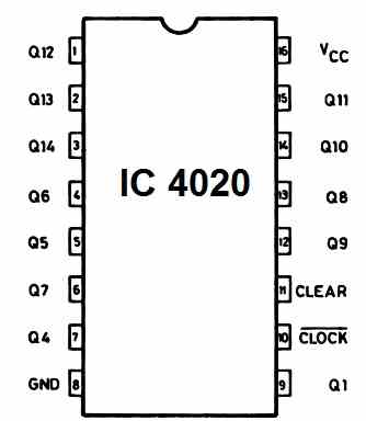
The IC 4020 has in all 16 pinouts.

Pin#16 is the positive supply input of the IC

Pin#8 is the ground supply or 0V pin of the IC.

Pin#10 is the Clock input pinout of the IC. This pin receives the clock frequency input

Pin#11 is the Clear or the reset pinout of the IC. This pinout can be applied with a positive high to clear the outputs to zero.

The remaining pinouts, pin#9, 7, 5, 4, 6, 13, 12, 14, 15, 1, 2, 3 are all outputs of the IC 4020.

Understanding the pinout function of IC 4020

The pinout working of the IC 4020 can be understood with the following points:

Q1 means, divide 2 to the power 1 = 21

Q4 means, divide 2 to the power 4 = 24

In this way, Q12 means, divide 2 to the power 12 = 212

Now, which frequency will be divided by the above explained pinouts? It is the input frequency at pin#10 of the IC, which is the clock frequency.

The clock frequency applied at pin#10 will be divided the respective output pins Q1, Q4, Q5, Q6, Q7, Q8, Q9, Q10, Q11, Q12, Q13, Q14.

For example, let's consider pin#4 which is Q6. Q6 = Divide by 26 which is equal to 64.

This implies that if the frequency at pin#10 of the IC is 64 Hz, then the pin#4 which is Q6 will generate a frequency of 1 Hz.

We get the result by dividing the 64 Hz frequency at pin#10 by Q4 output, which is equal to 26 = 64, that is 64/64 = 1 Hz. Therefore, Q4 will generate a 1 Hz frequency when 64 Hz frequency is applied at pin#10.

Applications

The main applications of the IC 4020 is as given below:

  1. Frequency division
  2. Timing delays
  3. Binary counting
  4. Clock generation
  5. Pulse generation
  6. Data counting.

You'll also like:

  • 1.  2N3904 Datasheet [40V, 200 mA NPN Transistor]
  • 2.  IC 4033 Pinouts, Datasheet, Application
  • 3.  IC LM7912, -12V Negative Voltage Regulator Explained
  • 4.  LM12 IC Datasheet, Application Circuits
  • 5.  High Current Triac BTA41/600B – Datasheet, Application Note
  • 6.  Comparator Datasheet Parameters

About Swagatam

I am an electronics engineer with over 15 years of hands-on experience. I am passionate about inventing, designing electronic circuits and PCBs, and helping hobbyists bring their projects to life. That is why I founded homemade-circuits.com, a website where I share innovative circuit ideas and tutorials. Have a circuit related question? Leave a comment.... I guarantee a reply!

Previous Post: « IC 4018 Datasheet, Pinout Function Explained
Next Post: IC 4026 Datasheet, Pinout Working, Application »

Reader Interactions

Comments

  1. Jedidiah says

    June 1, 2024 at 4:55 pm

    Am currently working on a project where by I need pre-set pulses, such that when the set sequence lapses, a buzzer beeps. Is this IC equal to the task?

    Reply
    • Swagatam says

      June 1, 2024 at 4:59 pm

      Yes, you can use IC 4020 or IC 4017 for the mentioned application…

      Reply
  2. Bruce Raggett says

    March 2, 2024 at 1:29 pm

    Hi again. Made the circuit ok but can not get it to trigger a simple transistor/LED circuit, 10k base and 470 ohm LED resistor, BC 547 transistor.
    Just like connecting base to ground but 2.5 volts show on multimeter?
    LED circuit is sensitive enough to trigger just by touch though when not connected to CD4020 circuit.
    Running circuit on 5v.
    Any ideas please.

    Reply
    • Swagatam says

      March 2, 2024 at 1:42 pm

      Your parts values have no problems, the LED must light up if there’s a logic high available from the IC output to 10k.
      Are you sure the 10k base resistor is getting a logic high from the relevant IC output?
      Please check the logic level from the IC at 10k, it should be around 5V, and the voltage across base/emitter of BC547 must be 0.6V.

      Reply
    • Bruce Raggett says

      March 3, 2024 at 4:00 am

      Got it. All the sample circuits for this chip that I have seen show output pins connected directly to a LED with no resistor, a 470 ohm is needed. Then tap off between the resistor and the output pin from the chip for a signal to other devices. This then works.
      Thank you for your time and trouble, much appreciated.

      Reply
      • Swagatam says

        March 3, 2024 at 9:21 am

        OK, thanks for the update.

        Reply
  3. Bruce Raggett says

    February 29, 2024 at 11:06 am

    Would a base resistor be needed between an output pin and transistor or logic gate chip?
    Thanks once again.

    Reply
    • Swagatam says

      February 29, 2024 at 11:17 am

      Yes, a base resistor will be needed between a logic gate output and a BJT base..

      Reply
      • Bruce Raggett says

        February 29, 2024 at 11:41 am

        Thanks ?

        Reply
  4. Bruce Raggett says

    February 29, 2024 at 9:14 am

    How do I use the reset function to start at “0” at power on and count from there?
    Momentery push button to “+” with a “pull down” resistor to “-“?
    Thank you.

    Reply
    • Swagatam says

      February 29, 2024 at 9:26 am

      If you want the reset function to be automatic, connect a 0.22uF capacitor between pin#11 and the positive line with a 100k resistor between pin#11 and ground. For manual reset just replace the 0.22uF with a momentary push button switch in the above setup.

      Reply
      • Bruce Raggett says

        February 29, 2024 at 11:04 am

        Thank you for that reply, exactly what I needed to know.

        Reply
        • Swagatam says

          February 29, 2024 at 11:16 am

          Glad it helped!!

          Reply

Need Help? Please Leave a Comment! We value your input—Kindly keep it relevant to the above topic! Cancel reply

Your email address will not be published. Required fields are marked *

Primary Sidebar

Subscribe to New Circuit Ideas

Categories

  • Arduino Projects (87)
  • Audio and Amplifier Projects (132)
  • Automation Projects (17)
  • Automobile Electronics (101)
  • Battery Charger Circuits (83)
  • Datasheets and Components (104)
  • Electronics Theory (143)
  • Free Energy (37)
  • Games and Sports Projects (11)
  • Grid and 3-Phase (19)
  • Health related Projects (25)
  • Home Electrical Circuits (12)
  • Indicator Circuits (14)
  • Inverter Circuits (87)
  • Lamps and Lights (142)
  • Meters and Testers (69)
  • Mini Projects (46)
  • Motor Controller (64)
  • Oscillator Circuits (27)
  • Pets and Pests (15)
  • Power Supply Circuits (108)
  • Remote Control Circuits (50)
  • Security and Alarm (64)
  • Sensors and Detectors (101)
  • Solar Controller Circuits (59)
  • Temperature Controllers (42)
  • Timer and Delay Relay (49)
  • Transmitter Circuits (29)
  • Voltage Control and Protection (37)
  • Water Controller (36)

Calculators

  • Battery Back up Time Calculator
  • Capacitance Reactance Calculator
  • IC 555 Astable Calculator
  • IC 555 Monostable Calculator
  • Inductance Calculator
  • LC Resonance Calculator
  • LM317, LM338, LM396 Calculator
  • Ohm’s Law Calculator
  • Phase Angle Phase Shift Calculator
  • Power Factor (PF) Calculator
  • Reactance Calculator
  • Transistor Astable Calculator
  • Transistor base Resistor Calculator
  • Voltage Divider Calculator
  • Wire Current Calculator
  • Zener Diode Calculator
  • Filter Capacitor Calculator
  • Buck Converter Calculator
  • Boost Converter Calculator
  • Solar Panel, Inverter, Battery Calculator
  • Wire Current Calculator
  • SMPS Transformer Calculator
  • IC SG3525, SG3524 Calculator
  • Inverter LC Filter Calculator

People Also Search

555 Circuits | 741 Circuits | LM324 Circuits | LM338 Circuits | 4017 Circuits | Ultrasonic Projects | SMPS Projects | Christmas Projects | MOSFETs | Radio Circuits | Laser Circuits | PIR Projects |

Recent Comments

  • Swagatam on How Shunt Regulator TL431 Works, Datasheet, Application
  • SA on How Shunt Regulator TL431 Works, Datasheet, Application
  • Swagatam on Timer Based Cell Phone Charger Circuit
  • Nitesh Agrawal on Timer Based Cell Phone Charger Circuit
  • Swagatam on Timer Based Cell Phone Charger Circuit

Company

  • Privacy Policy
  • Cookie Policy
  • About Me
  • Contact
  • Disclaimer
  • Copyright
  • Videos
  • Sitemap

Social Profiles

  • Twitter
  • YouTube
  • Instagram
  • Pinterest
  • My Facebook-Page
  • Quora
  • Stack Exchange
  • Linkedin
  • © 2025 · Swagatam Innovations