We all are pretty familiar with the 78XX voltage regulator ICs or the adjustable types such as LM317, LM338 etc. Though these regulators are outstanding with their specified functioning and reliability, these regulators have one big disadvantage.... they won't control anything above 35V.
Circuit Operation
The circuit presented in the following article introduces a DC regulator design which effectively counters the above issue and is able handle voltages as high as 100V.
I am a great admirer of the above mentioned types of ICs simply because they are easy to understand easy to configure and require bare minimum number of components, and are also relatively cheap to build.
However in areas where input voltages can be higher than 35 or 40 volts, things become difficult with these ICs.
While designing a solar controller for panels which produces in excess of 40 volts, I searched a lot over the net for some circuit that would control the 40+ volts from the panel to the desired output levels, say to 14V, but was quite disappointed as I couldn't find a single circuit which could fulfill the required specifications.
All I could find was a 2N3055 regulator circuit which couldn't supply even 1 amp current.
Failing to find a suitable match I had to advise the customer to go for a panel that would not generate anything above 30 volts...that's the compromise the customer had to make using a LM338 charger regulator.
However after some thinking I could finally come up with a design which is able to tackle high input voltages (DC) and is a lot better than the LM338/LM317 counterparts.
Let's try to understand my design in details with the following points:
Referring to the circuit diagram, the IC 741 becomes the heart of the entire regulator circuit.
Basically it has been set up as a comparator.
Pin#2 is provided with t a fixed reference voltage, decided by the value of the zener diode.
Pin#3 is clamped with a potential divider network which is appropriately calculated for sensing the voltages exceeding the specified output limit of the circuit.
Initially when the power is switched ON, R1 triggers the power transistor which tries to transfer the voltage at its source (input voltage) across the other side of its drain pin.
The moment voltage hits the Rb/Rc network, it senses the rising voltage conditions and within a fraction of a second the situation triggers the IC whose output instantaneously goes high, switching off the power transistor.
This instantly tends to switch OFF the voltage at the output reducing the voltage across Rb/Rc, prompting the IC output to go low again, turning ON the power trasistor so that the cycle locks in and repeats, initiating an output level that's just exactly equal to the desired value set by the user.
Circuit Diagram
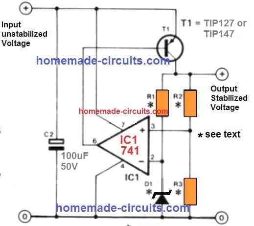
The values of the unspecified components in the circuit may be calculated by the following formulas and the desired output voltages may be fixed and set up:
R1 = 0.2 x R2 (k Ohms)
R2 = (Output V - D1 voltage) x 1k Ohm
R3 = D1 voltage x 1k Ohm.
The power transistor is a PNP, should be suitably selected which can handle the required high voltage, high current in order to regulate and convert the input source to desired levels.
You can also try replacing the power transistor with a P-channel MOSFET for even higher power output.
The maximum output voltage should not be set above 20 volts if a 741 IC is used. With 1/4 IC 324, the maximum output voltage can be exceeded up to 30 volts.
High Current Regulator with Low Dissipation
Power supply have been taken for granted since the introduction of the now-famous three-pin voltage regulators. However, there are times when such a regulator is insufficient. This sort of regulator requires a significant potential drop across it (usually greater than 3 V) and a high quiescent current (typically 6 mA for a 78xx). The regulator shown here is very appealing for battery-operated devices, as it provides:
- The output voltage is variable and highly steady.
- Reduced potential drop (some tenths of a volt).
- Quiescent current of a very small magnitude (20-30 uA).
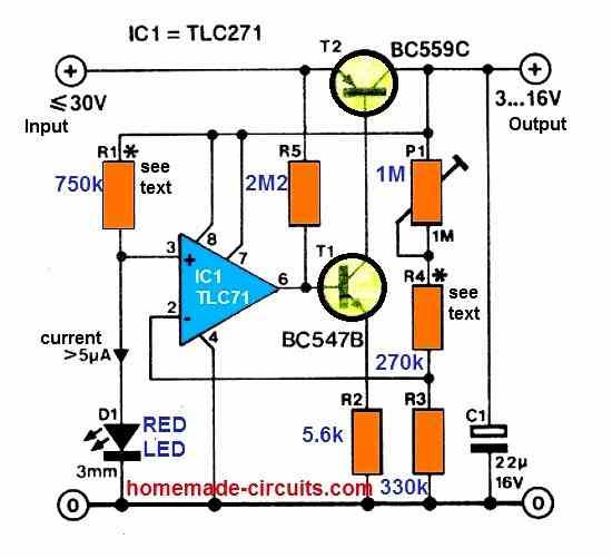
The regulator is a typical series type in theory. A common or garden red LED with a current demand of not less than 5uA is used as a voltage reference. An LED has a rather constant voltage drop at this modest current. The current is taken from the regulated output through R1. This improves the stability.
The TLC271 CMOS opamp provides regulation. By connecting pin 8 to the positive output terminal, this amplifier runs in the low bias mode, which assures extremely low current usage. The opamp's output is utilized as the basis drive for series regulator T2, which is driven by current source T1. This arrangement allows for good control of a tiny voltage swing at the opamp's output.
This is important because the opamp's slew rate in low-bias mode is rather low. The opamp gets its power from the regulator output as well. Capacitor C1 acts as a decoupling element for the opamp as a result. A type of bootstrap resistor, R5, was determined to be required for efficient control.
The settings of R1 and R4 in the diagram result in a 3 to 8 V adjustable output voltage. R4 can be increased by 200 k / V to get higher output voltages of up to 16 V. As long as the current through D1 does not decrease under 5uA, the value of resistor R1 must be raised as well.
Long connections in this sort of circuit should be avoided at all costs to avoid parasitic capacitances. The regulation would deteriorate as a result of this. The peak output current is primarily determined by the allowable dissipation in T2 and, to a minor extent, by the voltage difference between the input and output.


Comments
Dear Mr.Swagatam I have a stereo power amp 400 watts 100-volt power supply, one channel is already burned, I want to replace it with a 300-watt board but it’s working voltage only 60 volt maximum, how to reduce the supply. Thank you
Good evening Mr. Swagatam, I found your site searching for plans to build a HV Power Supply. I need a HV Power supply to use to kill rats in my garden. I have seen YouTube videos using stun guns (didn’t work) also using a 24V battery connected to a capacitor. The videos fail to list details or safety precautions. I have built an enclosure with aluminum strip electrodes, just need a HV power source. I just subscribed to your site a d would greatly appreciate any help you can provide.
Thankyou,
Greg Grimsley
Dear Mamad,
the ideal option would be to use single 60V power supply and feed both the channels, or modify the existing 100V power supply to produce 60V.
Reducing would requires a buck converter circuit
hi bro, i wanted to modify my old motorcycle horn (non battery type vehicle) since it had a classsic ”krrrr….krrrr” sound. i built a specific tone generator circuit using 555 and a mosfet to drive horn( may be diaphragm type). i also built a bridge using 3A diode for getting dc (2A/20v max) to my circuit from bike.Now everything is good but mosfet irf 840 (8A/500v) is getting excessively hot(without heatsink) and also same with 2n3055.
can u tell me how to how to prevent the mosfet from getting excessively hot? also which one u prefer for driving, mosfet or bjt?
bro, the heating cannot be prevented, and you will have attach to a heatsink to control it…for mosfet try IRF540, it will work better than IRF 840
Hi,
I have 18V 4A DC supply. Can I use this supply instead of transformer?
Hi, yes you can use it instead of a transformer based power supply
Hello sir help me I m 48 volt DC convert to 18 volt DC and 1am
use IC 7818
I might be missing something, but after searching the internet for how a p-channel mosfet works I can't see how this circuit could work except when the input voltage is very close to the output voltage (like within 1-3 volts). A p-channel mosfet needs gate to to raise up to the source to shut it off and this design holds it too low to ever stop it from conducting. The op-amp is driven from a much lower source voltage than the mosfet source so it can't shut it off – this design will just uncontrollably leak power from the input to the output. Also the Source/drain assignment compared to the chip drawing is backwards for a P-channel mosfet. Has anyone got this to work?
yes, it's rather a silly mistake in the diagram…the mosfet S/D needs to be reversed, with its source connected with the input supply.
I have discussed the concept elaborately in the following post, you can refer to it for an in-depth study:
https://www.homemade-circuits.com/2013/08/simple-zero-drop-solar-charger-circuit.html
I was looking for a motorbike regulator design and came across this. Has anyone got this circuit to work because I can't see how the op-amp can drive the mosfet gate voltage high enough to the source to turn it off so it would just seem to constantly conduct/pass. A p-channel enhanced mode mosfet typically has a source gate threshold of a 2-4 volts so if the op-amp can't drive the gate to nearly the input voltage, it cant shut it off and the op-amp is powered from a much smaller voltage so it can't get there. There needs to be a pull up resistor to pull the gate to the source voltage and the op-amp needs to drag that down which gives circuit start up issues so it'll never start-up.
I might have got this wrong but reading about a p-channel mosfet characteristic's on the internet I can't see how this can work at anything other than when the input voltage is very close to the desired output voltage – otherwise it will runaway and always pass the input voltage out to the output
Hi I would like to build voltage amplifier as well as regulator using lm741. The input would be 50 mv to 50 volt. The input pulses per min would be 1-30000. The output pulse should be regulated 5 volt at all frequencies and voltage inputs. There would be only +12 volt source for powering the op-amp & not the -12v. i.e the pin #4 will be grounded. the output from pin#6 would go to the micro-controller as it requires 5 volt. Plz if you could build the schematics for me.
you can try the first circuit as given in the following article:
https://www.homemade-circuits.com/2011/12/how-to-build-electronic-spy-bug-circuit.html
replace the MIC points with the input frequency and replace C2 with a 7805 IC.
Tx for the reply., but the issue is the battery bank is only of 12V not 48v. The input would be from 25 to 35v but the battery bank is only 12v. Hope to get a viable one.
…sorry the above link won't be suitable….you will need a BUCK converter circuit for this.
Please Google "buck converter circuit" you find plenty of them, use the one suits your application the most
OK, then you can try the second circuit from this link:
https://www.homemade-circuits.com/2011/12/how-to-make-simple-low-battery-voltage.html
Sir,
I need a good and stable ckt which can take input of 42V @ 20amps to charge a battery bank of 12V 400ah. Plz help me in this regards,
Kumar
kadimi You can try the following circuit:
https://www.homemade-circuits.com/2014/04/48v-solar-battery-charger-circuit-with.html