The simple configuration of a transformerless power supply circuit presented below is able to provide high current at any assigned fixed voltage level. The idea seems to have solved the problem of deriving high current from capacitive power supplies which earlier seemed a difficult proposition.
Introduction
I have discussed a few transformerless power supply circuits in this blog which are good only with low power applications, and tend to become less effective or useless with high current loads.
The above concept utilizes high voltage PP capacitors for dropping the mains voltage to the required level, however it is unable to raise current levels as per any desired particular application.
Although, since the current is directly proportional to the reactance of the capacitors, means the current can be lifted just by incorporating more capacitors in parallel.
But this puts a risk of high initial surge currents which might destroy the involved electronic circuit instantly.
Adding Capacitors to Increase Current
Therefore adding capacitors might help to increase the current specs of such power supplies but the surge factor must be first taken care of for making the circuit feasible for practical usage.
The circuit of a high current transformerless power supply explained here hopefully, effectively handles the surge developing from power transients such that the output becomes free from the dangers, and provides the required current supply at the rated voltage levels.
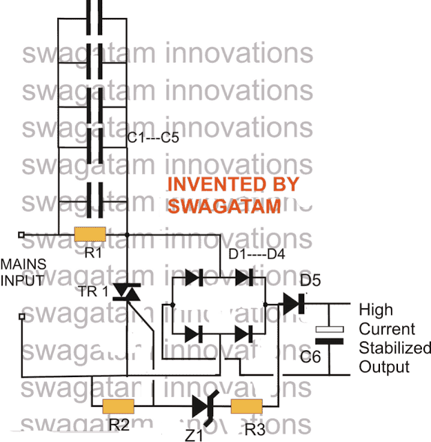
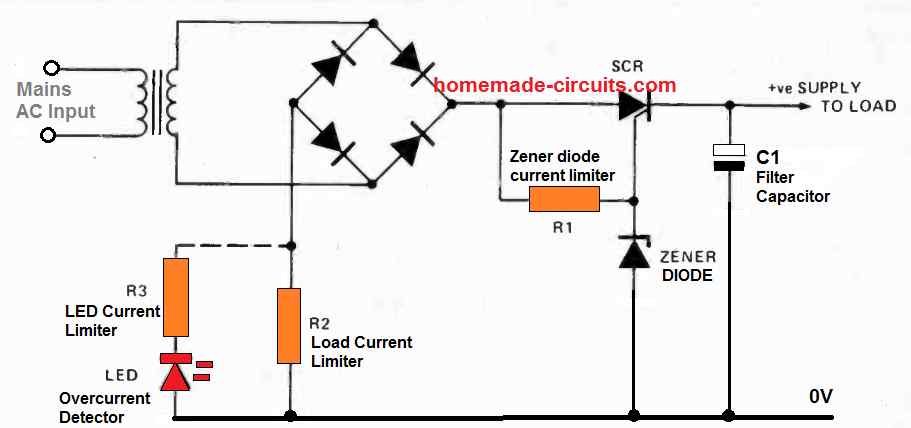
Everything in the circuit is kept just as its old counterpart, barring the inclusion of the triac and zener network which actually is a crowbar network, used for grounding anything that goes above the rated voltage.
In this circuit the output would hopefully provide a stable voltage of around 12+ volts at around 500 mA of current without the dangers of any accidental voltage or current influx.
CAUTION: THE CIRCUIT IS NOT ISOLATED FROM MAINS AND THEREFORE INVOLVES HIGH RISK OF ELECTROCUTION, APPROPRIATE PRECAUTION NEEDS TO BE EXERCISED.
UPDATE: A better and a more advanced design can be learned in this zero crossing controlled surge free transformerless power supply circuit
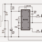
Parts List
- R1 = 1M, 1/4W
- R2,R3 = 1K, 1/4 WATT
- C1----C5 = 2uF/400V PPC, EACH
- C6 = 100uF/25V
- All DIODES = 1N4007
- Z1 = 15V, 1 watt
- TRIAC = BT136
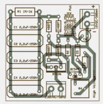
A neatly drawn PCB for the above high current transformerless power supply may be seen below, it was designed by Mr. Patrick Bruyn, one of the avid followers of this blog.
Update
A deeper analysis of the circuit showed that the triac was dumping a significant amount of current while restricting the surge and controlling the current.
The approach taken in the above circuit for controlling voltage and the surge is negative in terms of efficiency.
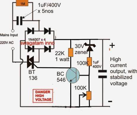
In order to obtain the intended results as proposed in the above design and without shunting precious amps, a circuit with exactly opposite response needs to be implemented, as shown above
Interestingly, here the triac is not configured to dump power rather it's wired in a such a way that it switches OFF power as soon as the output reaches the specified safe voltage limit, which is detected by the BJT stage.
New Update:
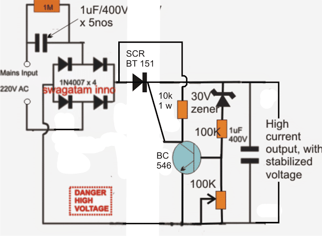
In the above modified design the triac may not conduct properly due to its rather awkward positioning.
The following diagram suggests a correctly configured version of the above, which can be expected to operate as per the expectations.
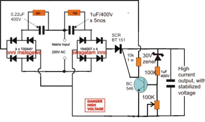
In this design we have incorporated an SCR instead of a triac since the positioning of the device is after the bridge rectifier and therefore the input is in the form of a DC ripples and not AC.
Improving the above design:
In the above SCR based transformerless power supply circuit, the output is surge protected through the SCR, but the BC546 is not protected.
In order to ensure a complete protection for the entire circuit along with the BC546 driver stage, a separate low power triggering stage needs to be added to the B546 stage. The amended design can be seen below:
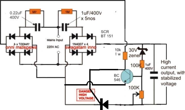
The above design can be further improved by modifying the position of the SCR as shown below:
So far we studied a few transformerless power supply designs with high current specs, and also have learned regarding their different modes of configurations.
Below we would go a little farther and learn how to make a variable version circuit using an SCR. The explained design not only provides the option of getting a continuously variable output but is also surge protected, and therefore become much reliable with its intended functions.
The circuit can be understood from the following description:
Circuit Operation
The left side section of the circuit is quite familiar to us, the input capacitor along with the four diodes and the filter capacitor forms the parts of a common, unreliable fixed voltage transformerless power supply circuit.
The output from this section will be unstable, prone to surge currents, and relatively dangerous to operate sensitive electronic circuits.
The portion of the circuit on the right side of the fuse transforms it into a completely new, sophisticated design.
The Crowbar Network
It's in fact a crowbar network, introduced for some interesting functions.
The zener diode along with R1 and P1 forms a kind of voltage clamp which decides at what voltage level the SCR should fire.
P1 effectively varies the zener voltage from zero to its maximum rating, so here it an be assumed to be zero to 24V.
Depending upon this adjustment, the firing voltage of the SCR gets set.
Supposing P1 sets a 12V range for the SCR gate, as soon as mains power is switched ON, the rectified DC voltage starts developing across D1 and P1.
The moment it reaches the 12V mark, the SCR gets sufficient triggering voltage and instantly conducts, short circuiting the output terminals.
The short circuiting of the output tends to drop the voltage toward zero, however the moment the voltage drop goes below the set 12V mark, the SCR is inhibited from the required gate voltage and it reverts to it non conducting state.... the situation yet again allows the voltage to rise, and the SCR repeats the process making sure the voltage never goes above the set threshold.
The inclusion of the crowbar design also ensures a surge free output since the SCR never allows any surge to pass through to the output under all circumstances, and also allows relatively higher current operations.
Circuit Diagram
Another SCR based Circuit
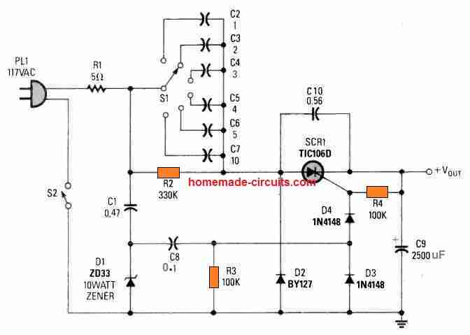
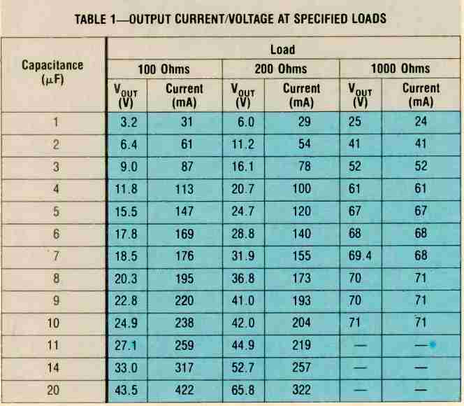
This SCR based high current Transformerless Power Supply consists of rather a few, easily accessible electronic parts.
The output voltage level (and also the level of feasible current as provided in the Table I) is adjustable by rotating the rotary switch S1.
Table#1
Zero Crossing Controlled High Current Transformerless Power Supply Circuit
The following circuit shows how a zero crossing concept can be implemented to create an effective transformerless high current power supply circuit, which is highly customizable.
Advantages of this Circuit are as follows:
100% surge free ensures that the load, zener diode and the capacitor are completely safe all the time regardless of the input switching conditions of the power supply.
No heat dissipation ensures that the circuit's efficiency is maximum.
How the Circuit Works
We know that the main issue with transformerless power supply circuit is the switch ON surge current, which happens due to the sudden peak AC entering the electronic circuit connected with the power supply.
This sudden in-rush voltage and current leads to the burning of the vulnerable electronic components attached with the power supply.
This means that, if the load is allowed to be switched ON whenever the AC waveform nears the zero crossing then such mishaps can be avoided.
The above circuit does exactly this.
The NPN TIP122 conducts only when the AC waveform is below the zener value.
When the TIP122 conducts the AC waveform is already within the safe range of the load and this safe voltage gets stored in the 1000uF capacitor for powering the load.
The process continues for each cycle and only when the AC peak has dropped down safely to the zener value, which keeps the load powered consistently, with an optimized voltage and current inputs.

Comments
Swagatam Sir, I wish to make a 15 V 80 A transformerless power supply. Can you help me in designing an appropriate circuit? It is required for solid stat cooling system.
Hi Ravi Kant,
12V 80 amp power supply is not possible using transformerless capacitive power supply concepts, for that you will have to use an SMPS design.
Sir, can you suggest me the circuit for SMPS design for 15 V 80 Amp power supply along with the components.
Hi Ravikant, I will design it soon for you and let you know…
Thank you
I have posted the required design under the following post:
https://www.homemade-circuits.com/how-to-design-customized-220v-smps-circuits/
Hi Swagatam,
Above circuit is intended for stabilized 12DCV, I need 9DCV one, what resistor value to replace for R2 & R3?
Hi Awak,
The first circuit may involve a lot of heat dissipation, therefore I would strongly suggest you to try the LAST circuit given in the above article, which is a lossless power supply:
https://www.homemade-circuits.com/wp-content/uploads/2012/08/high-current-losssless-transformerless-power-supply-circuit.jpg
Thank for response. The 1st circuit is high current one, IINW withstand for about 500mA. What about this one, if the cap I put 5 in parallel, can it be beared the same one?
Yes, it can handle 500mA or more easily because the MJE13005 is rated to handle upto 8 amps. The best thing about this circuit is that the transistor will not dissipate heat unnecessarily.
Sorry to my latest post, try to draw back my comment, but I can’t. A bit mistake read the schematic. It turns out to be have mylar capacitor.
No problem…. yes the 10uF/400V is the one which is mylar…
Swagatam,
I’m just aware, the schema doesn’t have mylar cap like the others, is that so?
Hi Awak, The 10uF/400V is the mylar capacitor.
Ok. Thank a lot.
hello sir. can mje13007 replace tip127 in the last circuit? thanks in advance. ops.. my mistake. mje13007 is npn transistor. but how about changing the pinout? is it posible to use npn transistor in this circuit?
Hello mbahsimak,
The previous diagram had some problems, so I have replaced it with a new one.
Now you can use MJE13007 instead of the shown TIP122….
allright, sir. I’ll be waiting the new circuit. thank you.
The circuit is already updated, please check it out.
one more question, is it allright if i use 4x 1n4007 instead of 6a4 diode?
Yes…and there’s no 6A4 in the updated design:
https://www.homemade-circuits.com/wp-content/uploads/2012/08/lossless-alternator-regulator.jpg
Sorry, yes the bridge rectifier has 6A4 diodes, which you can replace with 1N5408 diodes if the load is 300mA or above.
thank you, sir. what is the whatage of the zenner diode? I just want to replace a small transformer in portable radio with this one. mybe 300ma up to 500ma 5v.
You are welcome mbahsimak,
If you want to use it with 220V AC then I would recommend having aa series 5uF/400V capacitor with the input AC supply.
And please note that none of this circuits are isolated from mains AC and is therefore carry the risk of fatal electric shock.
zener diode can be 1 watt rated.
allright sir, i understand. but there is not enough place for 5uf/400v cpacitor in the portable radio. is it allright if i just use MB10S smd diode bridge (i can get it from led lamp) without capacitor?
mbahsimak, if you want to use it without an input capacitor then please include a 300mA fuse at the input side, just to make sure nothing burns in case something goes wrong.
sir ,2 phase 415v ac to 190v dc 6amp power supply ckt diagram.
sreenivasulu, how many wires do you have in your two phase system, please clarify this, I will try to help!
Hi sir, I need an inverter circuit that I can use with 0-24v (10amp) transformer
Thanks Majaha, I will try to suggest a proper design for you soon.
Hi Mr Swagatam , firstly I want to thank and praise you for tutorials in electronics engineering, they are very helpful and understandable.I want a circuit for reducing 230v ac to 120v ac(2amps).Looking forward for your response.
Thank You Majaha, I appreciate your kind words.
You can simply use a transformer with 230V winding at the primary, and 120V winding at the secondary for the required conversions.
Hi Swagatam,
do you think the zero crossing version you posted can handle 48vdc @ 1A ? Considering input voltage is 110Vac. Also, should I increase the input capacitor value or can I leave 2uF?
Cheers
Hi Cheerios,
Yes TIP127 is rated at 5 amp 100v, so 48v, 1 amp is within its reach.
However, for 1 amp current the input capacitor will need to be rated at 20 uF/ 250v
Thanks for your reply, do you think is it possible to use smd ceramic capacitors ?
Yes, you can use 20uF 250v smd capacitor if that’s avaliable to you…
What is the maximum current that your final circuit can withstand in its current state without modification? I want to charge an 18650 battery with a current that does not exceed 250 milliamps. Is it suitable in its current state?
Thank you man.
The last circuit using tip127 can handle upto 2 amps, but I am not sure if tip127 is suitable for this application, if it burns please consider using a 400v pnp transistor.
I designed the last circuit as is, without change, and it works very well. I put a zener diode as you did, but the output voltage was 21 volts, so I had to put another 5.6 volt zener diode on the exit capacitor, so there were 2 zener diodes in the circuit, and the circuit actually worked very well. The battery was charged perfectly, noting that the exit capacitor is 2200u 25v. My question to you is: Why was the circuit exiting before the last zener diode was placed? Can I delete the first zeber and leave the last zener? Or leave the circuit as it is with 2 zener diodes?
That’s great Hima, Glad the last circuit is working for you.
Which zener diode did you use at the base of the TIP127?
I think if this zener diode is adjusted appropriately then the second zener diode across the output capacitor will not be required.
Can you please try different lower value zener diodes until you get the 5V at the output.
Otherwise you can also try using many 1N4148 diodes in series to create the intended, equivalent zener diode at the transistor base.
Let me know how it goes.
My dear brother, thank you for your quick response to my message. Firstly, the value of the zener on the gate of the transistor tip 127 is 5.1 volts, but unfortunately it did not work well in charging the battery, and since I combined with your circuit another circuit to cut off charge, it was necessary to add a zener of 5.6 volts for precise calibration to disconnect the battery charge when… Voltage 4.2. Indeed, the integration of the two circuits together was successful, and four different types of 18650 batteries were charged. The charging was also separated perfectly at voltage 4.2, and no part in the two circuits heated up at all. I would like to thank you very much for what you provided on this site. I have another question there. Noise at the ceramic input capacitor. Is there a solution or not?
No problem Hima, if two zener diodes are working good for you, you can keep them as is.
The ripple noise at the input side cannot be eliminated, because if you connect a filter capacitor that will cause the tip127 to switch off permanently and the circuit will not work.
Thank you dear, how much current is the last circuit?
Hello Hima, the current capacity of the last circuit will depend on the transistor current rating, with a TIP127 it can be around 2 amps.
Hi Swagatam!
I must say these articles are very helpful.
I needed your opinion on the following idea for building a high current transformer less power supply.
We design it in two stages. The first stage, is a low current stage which just generates enough power for a small, low-cost, microcontroller with an ADC.
In the second stage, this microcontroller using the ADC and a MOSFET … samples the input AC and disconnects the AC as soon as the voltage goes above say Xvolts and below 0V. So the AC waveform gets clipped and rectified at Xvolts positive to 0V. Then we use a smoothing capacitor to generate the DC we want by changing the value of X in the firmware.
Since the MOSFET is controlled by the microcontroller… it is never switched on above Xvolts … so the surge etc. are all handled adequately.
The point is .. one MOSFET that can handle, say, 200mA of current at 300V, and a small microcontroller are still much cheaper (and easily available) compared to components needed in a high-performance SMPS power supply.
I built and tested this circuit and it works … I am just wondering why it is not used so widely.
Thank you Vineet,
May I know what is the current and voltage outputs of the concept that you built? Can you build a 12 V, 5 amp design using your concept. So that is the actual challenge, building a high current low voltage power supply without involving a transformer.
Let me know your thoughts on this.
I earlier designed two power supplies using flyback switched mode transformer based power supplies for two different projects …
48V 2A for a telecom product4V 600mA for a metering productAt that time I did not focus too much on making them tranformer-less … but while I was validating these designs, I played around with the concept I discussed and it worked. However, I did not invest too much serious time on it then.
Now I need to mass-produce another product and I am seriously looking at using the concept I proposed. But needed your opinion on this before I start allocating resources to it. Can you think of any reason it would not work … so I can think of some way to design better before I ask my team to start prototyping.
The mosfet would turn on when the AC voltage is just zero crossing towards positive, so there would be no stress. There could be some risk that the mosfet would disconnect at X voltage …(say 12V) … but I think since we are using a 300V mosfet … it should not have a problem handling that.
Your proposed concept is supposed to work using a microcontroller and without a transformer. However without a transformer high current generation may not be possible? If you think generating high current is possible, I would be interested to know. According to me SMPS is the only way to transform high AC voltage to a low DC voltage with the desired high current, efficiently.
The heat will depend on the input voltage and the output voltage difference. Since there’s a big difference between 36 V and 220 V, the heat will be also very high, there’s no way to reduce it.
how to overcome so that the scr is not too hot or becomes hot, thank you for the help, friend swagatam