The driver board EGS002 was created especially for single-phase sinusoid inverters.
It makes use of an IR2110S driver chip and an ASIC EG8010 control chip.
Protection against voltage, current, and temperature is included into the driver board.
LEDs are used to indicate warnings, and fan control is included.
Jumpers enable the setting of dead time, soft start mode, and 50/60Hz AC output.
EGS002, which is an enhancement over EGS001, keeps the original interfaces of EGS001 compatible.
In addition, cross-conduction prevention logic is included into EGS002 for improved anti-interference performance.
For user convenience, an LCD display interface is provided, allowing the chip's integrated display capabilities to be used.
Here are some general datasheet for the EGS002:
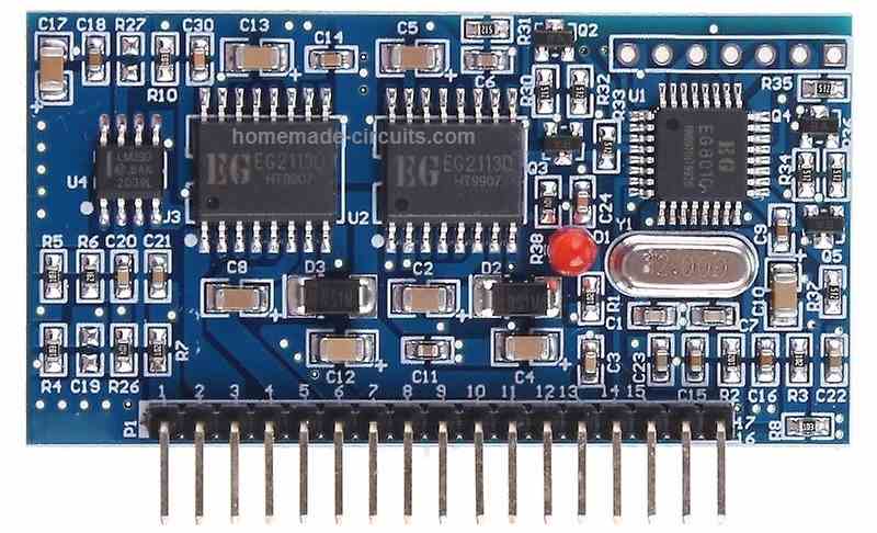
General Datasheet
- Input voltage range: +15V - +20V DC and +5V
- Output voltage range: 110V or 220V AC (depending on the transformer used)
- Output frequency: 50Hz or 60Hz (depending on the configuration of the chip)
- Maximum output power: approximately 300W
- PWM frequency: 16kHz
- Over-current protection: Yes
- Over-voltage protection: Yes
- Under-voltage protection: Yes
- Over-temperature protection: Yes
- Standby power consumption: less than 1W
The EGS002 is designed to work with a center-tapped transformer, and can generate a pure sine wave output waveform using a combination of PWM and SPWM modulation techniques.
It has a low standby power consumption, high efficiency, and comprehensive protection features that make it suitable for small-scale renewable energy applications.
Note that these specifications are general and can vary depending on the specific implementation of the EGS002 inverter board.
It's always best to consult the datasheet or technical specifications provided by the supplier or manufacturer for the specific board you are working with.
Circuit Diagram for External MOSFETs
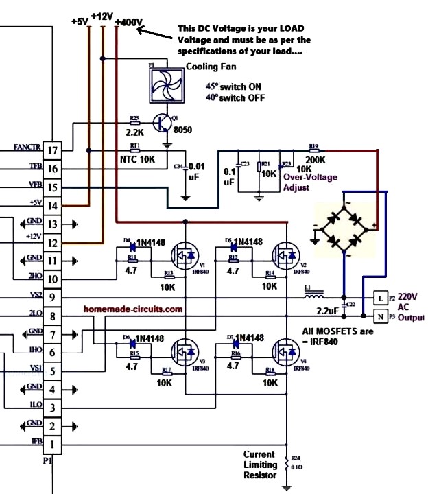
How to Connect
Connecting the EGS002 board to external MOSFETs is feasible, however it needs a few improvements to the board and good knowledge of the circuit design.
Listed below are the recommended methods to connect the EGS002 board to external MOSFETs:
Get rid of the present MOSFETs from the EGS002 board.
This would call for desoldering the MOSFETs from the board and eliminating any associated elements (for example gate resistors and diodes).
Choose the external MOSFETs that you would like to work with.
Ensure these are rated for the voltage and current specifications of your application.
Connect the gate of each external MOSFET to the equivalent gate drive signal on the EGS002 board.
The gate drive signals are generally named as "G" on the board.
Hook up the drain of each external MOSFET to the positive output of the center-tapped transformer.
The positive output of the transformer is normally attached to the positive terminal of the output capacitor.
Hook up the source of each external MOSFET to the negative output of the center-tapped transformer.
The negative output of the transformer is usually attached to the negative pin of the output capacitor.
Insert any essential elements to the circuit, for example gate resistors and diodes, to guarantee correct functioning of the MOSFETs.
Customize the control jumpers on the EGS002 board make it possible for external MOSFET functioning.
This might demand modifying the jumper settings for the "EGS002/04" and "EGS002/05" pins on the board, along with setting up the "EGS002/01" jumper to "ext".
It is critical to remember that changing the EGS002 board in this manner could be complicated and necessitates a great knowledge of the circuit design.
If you are not knowledgeable in electronics or inverter design, it's best to speak with an experienced person or work with a pre-built inverter board that actually contains external MOSFETs
LED Warning Indicator
The EGS002 driver board is equipped with an LED warning alert feature that assists users in identifying potential issues based on the following patterns:
- Normal Operation: The LED remains continuously illuminated.
- Overcurrent Condition: The LED blinks twice, then turns off for a 2-second interval, repeating in a cyclic manner.
- Overvoltage Situation: The LED blinks three times, followed by a 2-second off period, and then repeats this cycle.
- Undervoltage Problem: A sequence of four LED blinks occurs, succeeded by a 2-second pause, and the cycle continues.
- Overtemperature Issue: The LED blinks five times, pauses for 2 seconds, and maintains this cyclic pattern.
Pin Description and Working Details for EGS002
| Pin | Name | I/O | Output Current Feedback/Descriptions |
|---|---|---|---|
| 1 | IFB | I | Pin voltage exceeding +0.5V triggers overcurrent protection |
| 2 | GND | GND | Ground |
| 3 | ILO | O | Right H-bridge Low side MOSFET gate driver output |
| 4 | GND | GND | Ground |
| 5 | VS1 | O | Right H-bridge high-side gate driver return path |
| 6 | 1HO | O | Right H-bridge High side MOSFET gate driver output |
| 7 | GND | GND | Ground |
| 8 | 2LO | O | Left H-bridge Low side MOSFET gate driver output |
| 9 | VS2 | O | Left H-bridge high-side gate driver return path |
| 10 | 2HO | O | Left H-bridge High side MOSFET gate driver output |
| 11 | GND | GND | Ground |
| 12 | +12V | +12V | +12V Input DC voltage input, can be between 10V-15V. |
| 13 | GND | GND | Ground |
| 14 | +5V | +5V | +5V DC supply |
| 15 | VFB | I | AC output voltage feedback to regulate the output voltage, requires +3V to activate. |
| 16 | TFB | I | Temperature monitored with overtemp protection at +4.3V pin voltage |
| 17 | FANCTR | O | Temperature-controlled fan. FANCTR turns the fan on (high output, 1) when above 45°C and off (low output, 0) below 40°C. |
Pinout for LCD Display Connection
| PinOut | Name | I/O | Description |
|---|---|---|---|
| *1 | +5V | Power Input | LCD power supply |
| *2 | GND | Ground | Ground connection |
| *3 | LCDDI | I/O | LCD serial data |
| *4 | LCDCLK | Output | LCD serial clock |
| *5 | LCDEN | Output | LCD chip select |
| *6 | LED+ | Power Input | Backlight power supply |
| *7 | LED- | Ground | Backlight ground connectionpen_spark |
Jumper Setting Details
| Designator | Name | Mark | JP jumper shorted selects [setting description] |
|---|---|---|---|
| 1 | FS0 | JP1 JP5 | JP1 shorted sets AC output to 60Hz Shorting JP5 sets the frequency to 50Hz |
| 2 | SST | JP2 JP6 | JP2 short enables 3s soft start JP6 short disables soft start |
| 3 | DT0 | JP3 JP7 | JP7+JP8 shorted: dead time 300ns JP3+JP8 shorted: dead time 500ns |
| 4 | DT1 | JP4 JP8 | JP4+JP7 shorted: dead time 1.0us JP3+JP4 shorted: dead time 1.5us |
| *5 | LED+ | JP9 | JP9 short: LCD backlight ON JP9 open: LCD backlight OFF |
Default Jumper Settings:
- Output Frequency: 50Hz (JP5 shorted)
- Soft Start: Enabled (JP2 shorted)
- Dead Time: 300ns (JP7 and JP8 shorted)
Jumper Customization:
These jumpers can be manipulated or changed as per users specific needs.
Note:
- Avoid Shorting Conflicting Jumpers: Only one jumper per function can be shorted at a time. For example, you cannot short both JP1 (60Hz) and JP5 (50Hz) simultaneously.
How to Test EGS002 Driver Board
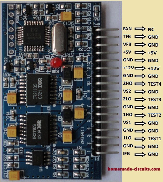
Initial Setup
- Grounding Test Points: During testing, connect the following pins to ground: IFB, VS1, VS2, VFB, and TFB.
- Power Supply Connections:
- Connect +5V DC to the +5V pin.
- Connect +12V DC to the +12V pin (voltage range: 12V to 15V).
Testing Procedure:
Waveform Observation:
- Connect an oscilloscope to test points TEST1 through TEST4 to check the waveforms.
- TEST1 & TEST2: Output fundamental frequency square wave (appears as the blue CH1 waveform in Figure 5-3).
- TEST3 & TEST4: Output unipolar modulation wave. When connected to an RC filter, these points will output the waveform shown as the red CH2 waveform.
Undervoltage Protection Test:
- Since the VFB pin is grounded, the undervoltage protection will activate after 3 seconds.
- This will cause TEST1 through TEST4 to shut down.
- An LED will blink four times, then turn off for 2 seconds, and this cycle will repeat.
- Reconnecting the EGS002 to the power supply will allow you to observe waveforms for another 3 seconds before the undervoltage protection activates again.

Questions & Answers
Hello,
Would it be a good idea to put blocking zener diodes in parallel with the gate-drain resistors?
Regards.
Hi, zener diode can be added, but I recommend them across MOSFET gate/source, parallel to the 10k resistors.
Hi,
Yes, gate-sorce.
My mistake.
Thank you.
podrías pasarme algún diagrama para ésta targeta egs002
Sorry, I don’t have the full card circuit diagram, but you can easily replicate it using Arduino, as explained in the following article:
https://www.homemade-circuits.com/making-an-egs002-equivalent-board-using-arduino/
Can I directly take the VFB input from ac line terminal without rectifying? many schematics show it using rectifier then inserting it to VFB. if my h bridge gets less than 400v? like 320/350, can that cause issue?
Thanks very much for indicating this critical error in the diagram, yes the VFB requires an external rectification to DC before applying to the EGS002 VFB pin….I have now corrected the diagram, please check it.
The +400V indicated in the diagram is the load specific voltage, it must be as per the specifications of the load….for example if your load is 220V then this DC bus voltage on the MOSFETs drain will need to be 310V DC….
meaning this bus voltage must be equivalent to the peak voltage specification of your load.
Hello, I adapted an EGS002 to a 72V 4000W Unizuky inverter, and two IGBTs are getting hotter than the other two. The inverter is delivering 110V and 60Hz, which is correct, but I’m concerned about the heat. Could the overheating be due to the UFB reference being drawn from the unrectified AC output? Any help would be greatly appreciated.
Hi, did you use the exact H-bridge configuration shown in the above article? Are you using a well designed PCB with short tracks for the H-bridge devices?
I’m actually confused, in the original eg8010 datasheet, there is no rectifier. even electronoobs made one without the rectifier. and I’m struggling with finding a 3.3mH Inductor I have a 1.2mH one, can I pair it up with 4.7uF C ? i know it may increase the reactive current
No, you MUST add an external rectifier for the VFB pin, because the EGS002 boards do not have an internal rectifier for its VFB pin.
For the output AC side LC circuit, you can use the following calculator for optimizing the values:
https://www.homemade-circuits.com/inverter-lc-filter-calculator/
Hi everyone, I am working on a single phase inverter project using the EGS002 / EG8010 driver board.
I followed the typical application circuit from the datasheet/manual which shows a high voltage DC bus, around 400 V and a voltage feedback circuit for the AC output.
Because of that, I originally made my VFB voltage feedback circuit using that higher voltage level.
But, in my actual prototype test, I am now using only 12 V DC on the H bridge.
My question is: could this make the EG8010 think that the VFB pin is too low, almost as if it were grounded and so trigger the undervoltage protection after a few second then?
At first, I used the feedback resistor value shown in the reference circuit, around 200 kΩ.
Since I became aware that my test voltage was much lower than the voltage used in the datasheet example, I tried replacing that resistor with 10 kΩ to increase the feedback voltage going to VFB.
But, the circuit still did not work correctly, so now I am not sure if:
1. my feedback divider is still not giving correct voltage to the VFB pin
2. I am sampling the voltage from wrong point of the circuit
3. the EGS002 expect feedback from the final AC output after transformer/filter, not directly from the low voltage H bridge side
4. just changing the 200 kΩ resistor to 10 kΩ is not enough because the whole VFB feedback network needs to be recalculated.
From what I understand, EG8010 expect VFB signal to be around correct internal reference level during operation.
If the feedback voltage is too low, then it may spot undervoltage and shut down the SPWM outputs.
Could someone help me understand correct way to design VFB feedback circuit when testing H bridge with only 12 V DC then?
What voltage should I measure at the VFB pin during normal operation and how should I figure out the resistor divider for a low voltage test setup?
Any doable solution or correction would be very helpful, thanks in advance…
Please Engineer, building 3kw-24v inverter, using 24 Hy4008 mosfets, now problem is, when you buy the Egs002 module, it has factory dead time setting on 300ns, what should be the precise dead time setting for my 24 mosfets build, for effective working of the transistors without frying them.
Actually, there is no precise dead-time value based only on the number of MOSFETs. For 24 HY4008 MOSFETs, 300ns may work but because you have several MOSFETs in parallel, so the total gate charge is much higher and the gate driver must be strong enough. I would start with 500ns and check the gate signals with an oscilloscope. If the MOSFETs are fully OFF before the opposite side turns ON, 300ns can also be used. Do not select 1us or 1.5us just because you have 24 MOSFETs… because too much dead time can cause waveform distortion and extra heating.
Hi Yes, your intuition is 100% correct.
Now the EG8010 is shutting down because of its built in Undervoltage Protection (UVP).
Because you dropped the H bridge voltage from 400V to 12V without changing the feedback loop layout, chip thinks the inverter output has collapsed and kills the push after a few seconds.
Here is why it is happening and how you can fix up it: The VFB pin (Pin 13) expects a feedback signal that sits right around 1. 5V AC RMS (peaking near 3V), if it stays below roughly 0 then, 5V for more than a few seconds, protection triggers.
Dropping your bus to 12V dropped this feedback to near zero.
You must sample feedback from the final filtered AC output after the LC filter (inductor and capacitor), not directly from the H bridge switches.
H bridge output is stream of raw square pulses which the pin cannot read properly.
Just swapping the 200k resistor to 10k fails because the EGS002 feedback path isn’t a basic two resistor divider it also passes through a rectifying diode, filter capacitor and the onboard blue trimming potentiometer.
Two ways to solve this for your 12V test setup: Option A (Easiest for bench testing): If you just want to test your H bridge switching without shutdowns, then completely unhook AC feedback line and apply a steady, external 1. 5V DC (like from a battery or separate variable power supply) directly between the VFB pin and GND.
This tricks the chip into thinking everything is perfect so it stay running.
Option B (For true 12V feedback regulation): Route your low voltage H bridge output through an LC filter to get a clean, low voltage sine wave (around 8V to 9V AC RM).
To fall this safely to 1. 5V for the pin, your upper feedback resistor should be changed to roughly 47k to 50k (assuming the lower divider resistor is 10k).
From there, fine tune blue onboard potentiometer until the circuit stabilize.
Hello
Can 220 volts be connected directly to pins 5 and 9?
pls how can I connect egs002 with external gate driver to drive so many power MOSFET (20 power MOSFET or etc) for a 5kva inverter without burning the module. pls show me with label diagram
The EGS002 output can deliver upto 2amp source/sink current which is enough to drive many high power MOSFETs in parallel for building upto 5kva inverters, so no need of any external drivers…
Hi, yes, it can be connected as shown in the diagram…
L1 value?
https://www.homemade-circuits.com/inverter-lc-filter-calculator/
Can the EGS8010 also support transformerless design. I could not find it on the datasheet
resistors diode connection to mosfet pins is difficult convert to pcb board if you draw roughly a simple pcb good for beginners.
The diagram shown in the above article is transformerless…
Eu não entendi de onde vêm os 400 volts e de onde saem da placa os 220 AC! O restante ficou magnificamente ótimo.
The 400V is your source voltage with which you would want to operate the load. It can be from a solar panel, battery or any other similar source.
220V is acquired between the MOSFET junctions, as shown in the diagram…
Please can you tell me where do you connect the ground of 400vdc ? it shouden’t be connected to the ground of EG8010 ?
All grounds or negatives will be in common, meaning the -400V of the solar panel or the battery will also connect with the common connections of all the ground symbols, shown in the diagram…
great, thank you
I want to generate a pure sinusoidal waveform using Arduino to create a spwm signal. I have also built the circuit in Proteus. But the output may be shows a square wave and it is not stable.
I saw your full H-bridge inverter circuit . I mainly built that circuit, but I did not use BJT. I also use a LC(C=4.7uF and L=2mH) filter and a 12V/220V transformer.
In my project, I need to demonstrate both 50 Hz and 60 Hz. If I use modules, the main purpose of the project will not be fullfilled. I really don’t understand what to do now. If the software implementation is already in such bad condition, I don’t know what the hardware situation will be like. my arduink code is- #include
#include
// Sine Table – 50 samples for half wave
int sineTable[] = {0, 25, 50, 75, 99, 122, 144, 165, 184, 201, 216, 228, 238, 245, 250, 253, 254, 252, 248, 241, 232, 221, 208, 193, 176, 158, 139, 119, 98, 77, 56, 35, 14};
volatile int index = 0;
volatile boolean halfWave = true;
void setup() {
pinMode(9, OUTPUT);
pinMode(10, OUTPUT);
// Timer 1 configuration for high speed PWM
TCCR1A = 0b10100001; // Phase Correct PWM
TCCR1B = 0b00000001; // No prescaling
// Timer 2 for Sine frequency (50Hz)
TCCR2A = 0b00000010; // CTC Mode
TCCR2B = 0b00000100; // 64 prescaler
OCR2A = 62; // Approx 50Hz timing
TIMSK2 |= (1 <= 32) {
index = 0;
halfWave = !halfWave;
}
}
void loop() {
// Main code stays empty
}
Did you try the following concept, please try it exactly as given in the following post, along with the code:
https://www.homemade-circuits.com/making-an-egs002-equivalent-board-using-arduino/
You can ignore the opto coupler stage…
Good evening sir. thanks for your teachings.
my question is, can egs002 work with 16×2 LCD?
hola, I need help, I am interested in making an inverter with egs002 with a 110V /60Hz power transformer, I already made the basic circuit and managed to calculate the VFB adjustment R so that at its output it has the necessary 3 V, I am using a transformer UPS power from 12V to 110V and I can’t get the inverter to give me an AC voltage higher than 20V, I need some guidance or ideas to solve the problem, early greetings,
input+400v connection is ok but for the same negative is not showing in this diagram should be low side both mosfet between is correct place.
All the ground symbols must be connected together, which are also the common negative battery line…
Hi, If you are using the full bridge design as shown in the above article, then please do the following checks:
Disconnect the feedback link completely and check the voltage.
Make sure the MOSFETs are connected correctly.
Use 12V supply at the point where 400V is written in the diagram.
Check the voltage between each vertical half-bridge MOSFET source/drain node and the ground line…it must be 6V (50% average of 12V) check for both the half bridge sides….
Also check frequency across these points…
Hi Nnadi, yes it can, I will publish the full drawing and article soon for you in one day…keep in touch
hello, good morning, I have a question. Is there a way to reprogram the firewere of the EG8010 so that the LCD display can correct the sampling parameters when the circuit works at 110V AC since the reading that this parameter has is incorrect
Hi, I don’t think the EG8010 can be reprogrammed.
Instead you can design your own equivalent board using Arduino or Atmega
thank you so much. I will be waiting for that
No problems….here’s the link for your reference:
https://www.homemade-circuits.com/can-egs002-work-with-a-standard-16×2-lcd/
what do i do to make it work properly on heavy loads,because i have a strong transformer but it keeps of blinking 2 times and shut off
Only upgrading the transformer will not help, you must upgrade battery power and MOSFET power also, accordingly…
If i can use H20R1203 IGBT DC input around 260v DC output if i can gate 220v AC how many watt load capacity if i can use indction 1.5 Hp submarsuble water pump
Yes, H20R1203 IGBT can be used for this type of inverter, but 260V DC is not enough for getting proper 220V AC sine wave output. For 220V AC normally DC bus should be around 310V or more. Also 1.5 HP pump is around 1.1kW motor, but starting current is much higher, so inverter should be at least around 1.5 to 2kW with proper heatsink and protection. And IGBT gate needs proper gate driver, you cannot give 220V AC directly to gate.
How is the current in the circuit set so that the MOSFET or IGBT of the inverter does not blast? How is the current sense set?
You can use a DC shunt and OpAmp to build a overcurrent protection. For example if you want the inverter should shut off at 50A DC, then purchase a 50A/75mv DC shunt easily available online or at local market. Use an OpAmp to convert 75mv to 0.5V. Then output of thiz OpAmp ( which is at 0.5V) is connected to pin. 1 of EGS002. As per data sheet of EGS002, overcurrent operate af 0.5V at pin. 1.
If you want specific schematic DM me to testinghvdc@gmail.com
The current sensing resistor R24 gives that protection to the circuit, you can calculate and set it as per your max load current specifications…
saya sudah menghabiskan 4 modul egs.modul egs cuma cocok buat low frekuensi.untuk hing frekuensi out 220volt tapi untuk HZ keluar 90hz udah berbagai cara tetap di atas 60hz
hi where do you get the 400dc volt from . a Boost converter or ?
400V DC can be from a solar panel, or a battery bank…
sir solar inverter hardware software requirement
Sanwar, please provide detailed specifications of your requirement, i will try to figure it out….
for a full bridge 12v design what should be the transformer voltage
0-12V / 220V
are pins vs 1 and vs 2 directly connected to high volts in high frequency inverters?should you be given a rediator?
Pin1 goes to the current sensing resistor, pin2 goes to the supply negative or the 0V line of the DC supply…
HI PLEASE CONFIRM INDUCTOR L1 DETAIL
Hi, you can try the following calculator and customize the filter as per your needs:
https://www.homemade-circuits.com/inverter-lc-filter-calculator/
I have 0-9v won’t it work ?
It will work…with proportionately higher secondary side output voltage…
okay I have reconfigured to 12v
OK, great!
Hi, I’m from Russia. My name is Valera. I have a problems with SGE002. I have to got AC220v from use DC12v use this device, but I have got only out 110-115 v AC, I have used different transformers like 7/220 and 12/220 , and have same results. I would like to know where is fault. This device don’t have a jumper 110v to 220v. I ‘ve tried to change resistors ih VFB, no results.
Sincerely yours
Hi Valera, i have been following this site and all the problems you guys get with this design. Use a 24v battery and you will get 240+ v , just make sure to adjust the “over voltage adjust” variable resistor attached to VFB to match 50hz. a Good way to do this is put a frequency counter on your output and a use a adjustable DC supply. Use the 2 togehter to adjust volt and frequency to match 240v / 50hz
Hello, I had the same problem with this module and it was about the signal reaching one of the H-bridge MOSFETs. Another problem that appeared for me was high no-load current consumption in the transformer
Utilize transformador de Nobreak, 12 ou 24Volts para 220v, em 12 volts em cada Braço do Trafo, deve receber 7vots alternados, já para 24volts, deve receber 14volts.
quem determina a tensão é o TRafo.
Hi Valera,
Initially try by removing the feedback link completely, which connects with the VFB pin of the IC and check the results. Meaning let the VFB pin remain open and unconnected….
Check the transformer output without any load connected…
how to parallel the MOSFETs in 3x and do I need to put resistor 10k ohms and 10 ohms each MOSFETs that are parallel or it is parallel only the MOSFETs? like is it does the MOSFETs need snubber circuit
No need to put separate resistors for the gates of the MOSFETs, just connect the 3 terminals of the MOSFETs together in parallel, that’s all.
Yes, snubber may be required across the drains and sources of the combined parallel mosfets.
Hello Swag,
It is a new try for me to use EGS002 to make an inverter from 190VDC to 120VAC. I have met with difficulties: The driving signals for the four MOSFETs were correct as shown in the Application Notes, but AC output was swinging between 30-40V shown on an external monitoring voltmeter while the module-driven LCD display showed about 220V. During the above period an AC indicating LED bulb connected to the output was lighting but only for a couple of seconds, then the EGS002 flashed its red LED for “overvolage” alerting and stop outputing AC, followed by alerting “undervoltage”. This process would repeat for 4-5 cycles then stagged on undervoltage status. It could went into the same process by recycling the power. During this trial the MOSFETs V1,V3(driven by 2HO,2LO) broke twice to short-circuited, and the EGS003 itself also broke twice with its 2HO and 2LO respectively failed to output correct driving signals.
Could you or anyone else give me some help?
Fred
Canada
Hi Fred,
Mostly this kind of trouble happens because that EGS protection and real output sense are not matching or because MOSFETs are facing high voltage spikes due to no snubber or TVS, or because there is too small deadtime causing both MOSFETs to conduct together. Sometimes that heatsink or wrong pin connection can also short the drain. Also that 12V supply to EGS can be unstable and that confuses it. That is why we must go step by step.
First remove out all damaged MOSFETs and EGS module and replace with new ones. Check carefully that gate, drain, and source are connected correctly and that heatsink is not touching any drain. You must set jumper of EGS002 to 110V or 120V mode because if it stays at 220V then the module will think output is wrong and will trip protection. Also check that DC bus of 190V is stable and that EGS driver supply of 12V is not dipping or spiking.
Now before next test you must add few things. You put one small gate resistor maybe 10Ω or 22Ω and one pull-down resistor like 10kΩ between gate and source. Increase deadtime to safe level like few microseconds, connect one RC snubber across each half bridge to kill the spikes and one TVS diode or MOV across DC bus. You must keep all driver and power wires short and thick and put 0.1µF ceramic near EGS Vcc pin. You can also add soft-start resistor or NTC at DC input. Use MOSFETs that are at least 400V or 600V rated.
Then for test you remove any heavy load or LC filter and just use one small bulb. You power the system through one series resistor to limit current and you observe gate and drain waveforms. If you see big spikes then you stop and add stronger snubber or TVS. When the waveform becomes clean and stable then you can remove resistor and test on full power.
That EGS LCD is showing that theoretical value, not actual RMS. Your external meter is showing the real unstable output that is coming before the system trips. So both will not match during fault.
The reason those MOSFETs and EGS outputs got burnt is because those spikes or overlap currents killed them. So now you make all wiring neat, add all protections, increase deadtime, and use stronger MOSFETs. Then test again slowly.
Thank you very much, Swag, for your prompt and detailed reply. I will try again with more care as per your advice.
No problem Fred, I hope it gets solved soon..
I’m ordering new EGS boards. You mentioned earlier that I need to set the jumper for 120vac output, where is that jumper on the board,Swag?
Have a great day,
Fred
Sorry for the confusion Fred, Upon checking your EGS002 board images you sent me, it is clear that the EGS002 board does not have any 110V/220V jumper.

Some EGS005 versions have that option but EGS002 fixes the output using transformer ratio and feedback resistors.
So I can confirm that your output voltage depends on your transformer and the VFB resistor divider, not a jumper.”
Hey Fred, on some EGS005 boards, this jumper is the JP1 or JP2 header, located near the edge of the board beside the EG8010 chip. You will usually see two or three small pins with a removable shorting cap (jumper) on them.
If you put the jumper across the “220V” side, then board outputs 220–230 V AC (RMS).
If you put it across the “110V” or “120V” side, then it will output 110–120 V AC (RMS).
The exact position can differ slightly depending on the board version, so check the silkscreen text printed beside the pins — it might clearly say something like “JP1 → 110V/220V” or “J1 → AC Sel”.
Thank you Swag! My EGS002 boards have JP1 for 60Hz choice, and JP2 for 3 seconds soft start. Different than that you have, aren’t they?
Ah yes, you’re right Fred … some newer batches of EGS002 boards are a bit different. They no longer include the 110V/220V jumper. On those versions, JP1 is indeed for 50/60Hz selection and JP2 is for soft start enable or disable.
The output voltage selection (110V or 220V) in these newer modules is done through firmware or resistor configuration, not by a jumper anymore. The EG8010 chip actually sets the RMS output based on the internal voltage reference and feedback divider connected to its VFB pin, means that the board manufacturer preconfigures it.
So yes, your board version is slightly different from mine… yours already has the output voltage fixed at 220V by default (since most boards are shipped that way). If you need 120V output then you will have to modify the feedback resistor network or reprogram the EG8010 with a 120V firmware version, depending on your board design.
If you can share a close photo of your board (both sides) then I can confirm exactly which configuration you have got and how to adjust it safely.
I would have the photos attached to my previous message but I didn’t see how I could do that. Just now I attached them in my reply to the proxy email sender of your message: “Homemade Circuit Projects”, hoping it can pass them to you. Please let me know if I should use another way to send photos to you.
Thank you Swag,
Fred
No problem Fred, that email ID may not be the right one…
Please send it to my following ID, I will check it out and see if I can figure it out:
homemadecircuits
@gmail.com
Hello, I tell you that I wanted to use this module to repair a 4kw inverter, and I have only been able to put a charge of up to 1kw, and I need at least 2 kw. The issue is that when I put a 1700 kw charge the 220v voltage at the output fluctuates between 150 and 220v, it does not remain stable, I check the VFB pin and it maintains 2.8v without variation, and the LED on the card does not reflect any type of error
The problem may not be with the inverter and the feedback can do nothing in this situation, because here the output is dropping due to overload.
In that case I think you may have to upgrade the MOSFETs, battery and the transformer so that the output voltage does not drop and stays stable…
can you sell readymade inverter circuit
I want to buy
I can make it if it is large quantities…
Hello Mr. Swagatam, I would like to ask if I can use this module to create a frequency converter. I live between two countries with different frequencies: one 50Hz at 220V and the other at 60Hz at 120V (Brazil and Paraguay). So, I would rectify 220V and use the transformerless configuration with 120V output. My question is about the input voltage, which would be close to 300V, and also about the feedback circuit to control the output voltage. One project is for 80W, the other for 500W or 1000W. I appreciate any help! Thank you very much!
Hi Ed,
I think that can be dangerous.
A possibility could be to modify the internal SPWM of the EGS002 and then transform the 310V into an equivalent 120V or 160V peak sine wave, at the output.
So instead of EGS002 you can probably try an egs002 equivalent circuit such as the following one, since it allows you modify the SPWM and the final sine wave outcome… but this will require a thorough testing…
Thanks for responding so quickly! I’m considering using a 220V to 110V autotransformer, which is easy to find. This way, I can use the transformer to supply 110VAC 50Hz, which, after rectification, will go to 140VDC. Using it at the circuit output is also plausible, but they tend to be very poor in terms of efficiency. This project will be used in washing machines and refrigerators that only operate at 60Hz, so I’ll only power part of the appliance’s circuit, leaving the peripherals that consume more current to be powered by the 50Hz network. The project needs to be very low-cost and simple to build. I’ve seen several circuits online, but most are unstable, and others are very complex. This EGS002 module seems very reliable and inexpensive, and it can even have a display, which will make everything more professional. What do you suggest? once again, thank you!
You are right, however, an autotransformer can give 110V AC from 220V but it is not isolated, so handle it carefully. After rectification you will get around 155V DC, not 140V. For 60Hz operation, a small inverter using the EGS002 module is a better and safer choice. It is low-cost, stable, and gives proper 50/60Hz SPWM output, ideal for motor-based appliances.
hi Swagatam, I am trying to build a 2nd a inverter using EGS002 and mosfets IRF3205. I intend using 12 mosfets and I understand the IR2110s is not capable of driving the mosfets. I need a totem pole circuit to drive the . Please help me with a totem pole circuit.
Hi Suresh,
I guess you are referring to the circuit diagram discussed in the following article:
https://www.homemade-circuits.com/making-an-egs002-equivalent-board-using-arduino/
The problem is that a totem pole cannot be used on the high side due to the presence of bootstrapping, instead you can try a HCPL3120 based isolated gate driver option.
https://www.homemade-circuits.com/isolated-high-side-gate-driver-opto-coupler-hcpl3120-no-need-of-bootstrapping-capacitor-diode/
hello. greetings. Normally inverter manufacturers work with a 200Vdc or 210 Vdc buffer and from there convert the DC into 120V AC, in my case of analysis… I am working on an inverter and I would not like to go down to 170Vdc, I would like to maintain the voltage of 210Vdc to obtain 120Vac but with the egs002 I have not been able to achieve it, only with 170Vdc at 120Vac
Hi, how much output voltage do you get with 210V DC? Did to adjust the feedback preset to regulate the output to 120V AC??
With the egs002 module mounted and locking at 210Vdc, it gives me a 140Vac voltage output. When I try to make adjustments to the divider that delivers to the VFB pin of the egs002 module, what it does is trigger due to overvoltage as if the VFB pin were a limit and not a regulation.
The triggering at the over voltage threshold voltage is itself the regulation, since it keeps the voltage always below that higher threshold level. Please note that the over voltage regulator feedback is only designed to control the over voltage and NOT the under voltage.
How much voltage do you get with the feedback disconnected? If it is still 140V then the problem might be with your transformer or the PWM…
Dear Eng. Swagatam
I am profficanal maintenance for many electronic modern devices. There is other method without a transformer used in many devices for example UPS type APC. The designer used four Electra Coil instead of transformer and used IGBT full-bridge and two coil for each side, the control circuit is complex and 50Hz accurate pure sineware with capacitors connected for each side of bridge and output. can you please explain about this method and practical circuit because I want to build it to supply for some sentific devices.
my sincerely
Thank you Saad,
Yes this is a modern high frequency transformerless inverter design.
The coils you are mentioning are LC filter coils.
Here’s one example of such an inverter, but without LC filter, which can be designed if required, anytime by me.
https://www.homemade-circuits.com/arduino-h-bridge-sine-wave-inverter-circuit/
Hi Swagatam, i have a mosfet bridge board i extracted from a dead Victron 24v 5000w inverter and i want to use it with EGS002. The mosfet bridge board has gate driver IC’s HIP4082IPZ. Kindly help me with a diagram on how to go about it. Thanks in advance.
Darlington
Hi Darlington, I don’t think external MOSFET drivers can be added to EGS002 outputs, because EGS002 involves bootstrapping for the high side MOSFETs which might interfere with the external driver working…moreover the EGS002 itself has powerful drivers inside, so no external drivers may be required…
Thanks a lot for your reply so helpful