In this post I have explained a circuit which can be used for transforming an ordinary music into a music with depth and echo effects. Generating an echo effect electronically involves a process in which an input signal is extended and then mixed with the original signal to create collapsing decaying effect, which ultimately results in creating an echo like effect on the sound.
By Rana Das
Introduction
The standard method of digitally enhancing an audio signal to deliver an echo effect is by using some kind of delay line. This can produce a delay of between 100ms and 1 second, which is fed back to the input of the line for generating the echo effect.
The signal is subsequently fed several times, which gets weaker as the signal is supplied back to the input. This ultimately delivers a excellent example of a healthy echo and a very good audio effect. A distinct problem with this method is the cost of a delay line circuit.
A bucket brigade form of delay line, consisting some thousand delaying levels, is the cheapest technique however even with this approach the cost of the circuit may be quite high.
Nevertheless there can be a different option that is quite simple and cheap without a doubt. The tested results are generally not as nice as those using more modern strategies, that produce a genuine echo effect, but this can be a system really worth attempting if a true echo sound is not really achievable within your price range, or if you love tinkering with basic echo effects generator devices.
The idea is to chop the input signal and feed this signal back to the input. This may look easy but the condition is that the actual audio signal must have little bit of decay in it, otherwise this modified echo tactics might fail to produce the intended good effects.
For example, for voice signals which do not have sufficient decay, this circuit may not be able to process the audio perfectly to produce good echo effects, although the results might be still quite acceptable to many.
Basic Component Working
A basic echo effect design built around a MOSFET Q1 becomes the heart of the circuit, as can be viewed in the circuit diagram. A MOSFET provides a extremely high drain-to-source resistance when the forward gate bias is zero (or minimal), however this resistance falls to around 2ohms when a forward gate bias of a couple of volts is given to the MOSFET gate.
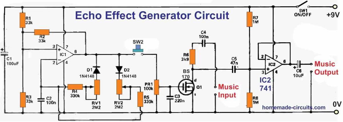
In this circuit a voltage controlled attenuator (VCA) is created through R6 and the drain/source resistance of Q1. You can find hardly any voltage drop via R6 when Q1 is turned off, because of the high input impedance of the buffer amplifier created through IC2 and the components connected around it. Therefore the audio signal reaches the output practically without any attenuation.
However as soon as Q1 is turned on by pressing SW2, a large quantity of the input voltage drops around R6 and a substantial degree of attenuation (normally around 66dB) is generated.
Despite the fact that this echo effect generator is pretty primitive type of VCA, it is sufficient for your current application, and is equipped with a significant edge over the majority of the more advanced options.
This is because our design produces no DC shift at the output while the circuit switches through the high attenuation condition to the low attenuation condition, and vice versa.
This feature eliminates the generation of "clicks" or "thuds" sounds that could definitely happen even when a tiny DC voltage shift was created by the circuit.
"Clicking" sounds may also be produced when the VCA was switched extremely fast between ON/OFF states so that the "chopped" signal are created with a very fast rise and fall periods. This could produce an incredibly abnormal effect, a lot better results could be achieved if the switching speed is slowed down slightly. This is exactly what C3 does.
The circuit is essentially a well-known and widely used arrangement, where IC1 is employed as the pulse generator circuit.
It differs from the normal circuit since here a couple of steering diodes D1 and D2 are involved in the timing circuit, resulting in independent timing resistances for the circuit's high and low output intervals. The low output period is controlled by R4 and RV1, whereas the high output period is controlled by R5 and RV2.
These two controls not only allow you to change the mark-space ratio of the control signal, but they also provide you a lot of flexibility over the pulse generator's working frequency.
The frequency range is around 2HZ when both the pots RV1 and RV2 are turned to minimal resistance and it is above 10HZ when both the pots are turned to their maximum resistance values.
SW1 disconnects the pulse generator's output from the VCA; Q1 is subsequently turned off, the input signal now travels directly to the output, causing the output effects to be disabled.
RV3 is required to match the pulse generator's output voltage swing to the circuit's required input specifications. This pot may be used to vary the achieved output effect to some extent since it is able to control the amplitude modulation depth. Because the circuit's current draw is not more than 4mA, a PP3 9V battery seems to be quite sufficient.
Circuit Description
The input signal first travels via a voltage controlled attenuator (VCA) and after this it travels through a buffer amplifier and to the output signal connector. The buffer amplifier is just required to guarantee that the device has a low output impedance and that the VCA output is not overloaded.
If the control voltage voltage is low, the VCA will give a direct and unrestricted path for the input signal, but if the control voltage is a few volts or larger, it will produce a rather significant amount of attenuation and essentially reject the input signal.
The control voltage is generated by the pulse generator stage, which has an output voltage that swings between practically negative supply voltage and almost positive supply potential, causing the VCA to switch between its minimum and maximum attenuation levels. This produces the necessary "chopping" of the input signal for the quasi-echo effect.
The pulse generator's high and low output timings may be separately tweaked using two potentiometer knobs RV1, RV2. These enable a reasonable level of control over the echo effect.
It also allows small bursts of signal to be permitted through the VCA, quick intervals to be created in the signal, or the on and off times of the signal to be about equal. These controls can be also used for adjusting the "chopping" frequency.


Questions & Answers
Do you have an Gerber version of this?
Thank you
Sorry Kim, I do not the PCB Gerber files for this project…
I have got the echo effect output for this circuit THanks you a lot…
Hey Swagitam,
Dan LL here. on some copycat site I saw a underground wire finder you published, but it was blurry and incomplete. Can you provide the url via email ? I love your site, it you ever need a 2nd contributor I’m a senior BSEE and I would love to help .. I’ve built a jillion projects. My 1st project dates me .. it was an Eico vacuum tube tester I still use. But I was only 6 or 7 when I built it, so don’t count me out sir !!!
Thank you Dan, I have actually already replied to this question in another article.
Never mind I will answer it again.
I am not sure if the following articles would help but this is all I have related to the underground wire finder designs:
https://www.homemade-circuits.com/stud-finder-circuit-find-hidden-metals-inside-walls/
https://www.homemade-circuits.com/deep-soil-metal-detector-circuit-ground/
Hope these help!
You are definitely welcome to contribute articles to this site, which are originally written by you and related to electronic circuits. I will be most happy to publish them here,
Hi Could you please tell me what the IC is?
Could we find it in ltspice?
Kind Regards
Hi, both the ICs are IC741, sorry I am not sure if it is available in LTSpice